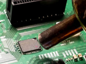
Traditional PCB Card Cloning
In the tradition process of PCB Card Cloning, it will be proceed in series of electronic design, layout design, Printed Wiring Board Manufacturing, measurement and debugging; in the Printed wiring board clone process, due to the absence of effective analysis measure and way on the real PCB card’s signal transmission; Pcb card cloning must be proceed according to the electronic component manufacturer and professions advice to proceed it. As a result of that, for a new clone project, normally will be very difficult to layout the signal topology structure and component parameter through the correct selection.
When the multiple digital signals on the PCB Board reverse engineering inspection need to switch, such as the CPU databus, address databus, due to the existence of impedance on the power supply line and grounding line, can generate the synchronized noise, on the grounding line can even have the surface ground reflected noise. The strength of SSN and ground bounce also depends the IO features of integrated circuit in the process of reverse engineering printed wiring board, impedance on the power supply plane and grounding plane, as well as the layout method.
Besides, same with other electronic device, PCB board copying also has the electro-magnetic compatibility issue, which also has a close connection with the PCB card layout and way of track arrangement.


