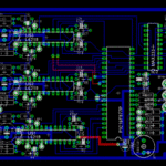
κλώνος pcb schematic
-
PCB Board Reverse Engineering Lay-Up
PCB Board Reverse Engineering Lay-Up structure will normally use P as the reference plane layer, S as the signal layer, T as top layer, B as bottom layer. Hereby we would like to take a PCB board with twelve layers as reference to illustrate the str...


