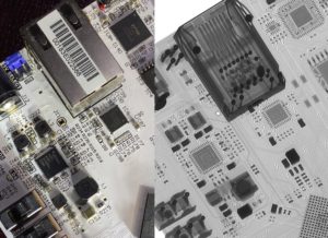
pwb duplicate
-
Printed Circuit Board Reverse Engineering Process
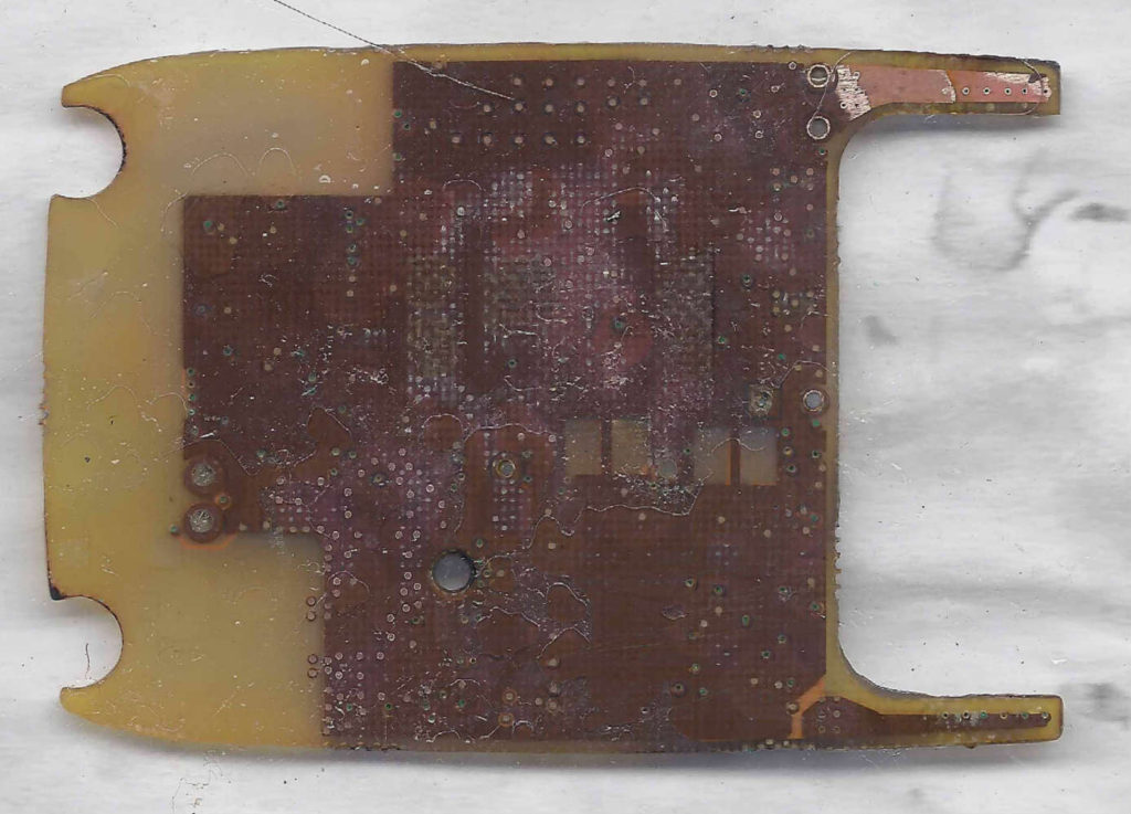
Simply speaking, Printed Circuit Board reverse engineering process include from electronic component dismount, list and rationally display them, scanning the TOP & BOTTOM layer, if multilayer printed circuit board need to scrub the surface to get...
-
Electronic PCB Board Reverse Engineering Service
In order to provide a better result for Electronic PCB Board Reverse Engineering Service, the try to make the distance between the hole distance and other components as much as possible, and standardize its dimension and optimize the processing thr...
-
PCB Board Reverse Engineering Schematic Diagram
PCB Board Reverse Engineering Schematic Diagram 1 Choose those components like integrate circuit, transformer and transistor with relative bigger size, has tremendous leads or playing important role at the PCB board as the standard part, and then sta...
-
Printed Circuit Board Reverse Engineering Power Comsuption
When there are multiple integrated circuits on the PCB Reverse Engineering, and some of them have great power comsuption, there will be great electrical level difference on the ground line and form the common impedance interference, In this case, it ...
-
Printed Wiring Board Reverse Engineering Manufacturing
Second step need to take the printed wiring board reverse engineering rule and limitation into consideration, if the PCB board reverse engineering task can be done smoothly, tools must work in the environment of correct rules and proper limitation. A...
-
Printed Wiring Board Reverse Engineering Pre-preparation Process
Printed Wiring Board reverse engineering process is undergoing a development process, accompany with the decreasing size of PCB Board dimension and increasing component density, PCB reverse engineering complexity level is raising up. How to realize t...


