Successive Approximation A/D Converter PCB Wiring Diagram Reverse Engineering
Successive Approximation A/D Converter PCB Wiring Diagram Reverse Engineering can help to extract circuit board layout drawing, Gerber file and schematic diagram, Bill of material from physical samples;

The successive approximation A/D converters have 8-bit, 10-bit, 12-bit, 16-bit, and 18-bit resolutions.
Initially, the process and structure of these converters was a bipolar type with R-2R resistor ladder network. But recently, these devices have been transplanted to CMOS technology using capacitive charge distribution topology.
Obviously, this migration does not change the system wiring rework strategy of these converters. Except for higher resolution devices, the basic wiring method is the same.
For these devices, special attention is needed to prevent digital feedback from the serial or parallel output interface of the converter.
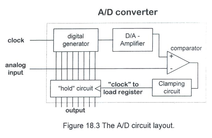
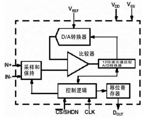
From the perspective of circuits and on-chip resources dedicated to different fields, simulation is dominant in successive approximation A/D converters. Below Figure is a block diagram of a 12-bit CMOS successive approximation A/D converter.


