12 Bit Sensing System PCB Board Wiring Diagram Cloning
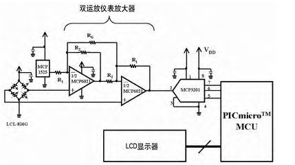
For 12 Bit Sensing System PCB Board Wiring Diagram Cloning, the applied circuit is a load cell circuit that can accurately measure the weight applied to the sensor, and then display the result on the LCD display.

The schematic diagram of 12 Bit Sensing System PCB Board being restored is shown in below Figure. The load unit used is LCL-816G from Omega. The LCL-816G sensor model is a bridge composed of four resistance elements, which requires voltage excitation.

The 5V excitation voltage is applied to the high end of the sensor, and when 900g maximum excitation is applied, the full-scale output swing is ±10mV differential signal.
This small differential signal is amplified by a dual op amp instrumentation amplifier. According to the circuit precision requirement, choose a 12-bit A/D converter. After the converter digitizes the voltage at the input, the digital code is sent to the microcontroller via the converter SPI port.
Then, the microcontroller uses a look-up table to convert the digital signal from the A/D converter into weight. At this time, if necessary, linearization and calibration can be implemented by the controller code. After completing this step, the results are sent to the LCD display.
The last step is to write the firmware for the controller. After the circuit is designed, the printed circuit board and wiring can be designed.

