Route Layout Drawing of PCB Reverse Engineering
There are a lot of routing tools, such as Autoroute, that are very tempting to use when routing the board. It is very important however that at least the important nets are routed by hand, and after autorouting, you must change some nets around and make sure everything is optimised. To auto route select Auto → Autoroute Board. To unroute the board, the sequence is Auto → Autounroute Board.
There is also a way to “fanout” the board, and place vias to ground everywhere a ground is needed. To do this go to the nets spreadsheet and disable all nets, except for ground, and choose Auto → Fanout Bard.
There are two different manual routing tools to use, and they both behave quite differently. These tools are “Add/Edit Route mode” and “Edit Segment Mode”. I personally use the Edit segment mode more regularly, however both have their benefits. They will also take some getting used to, so play around with them and figure out what mode you prefer to use.
If you right click while you are in either mode, there is a list of choices to unroute certain traces. Again personal preference will play a large factor when routing a board. Manually routing takes some getting used to, however once you make a few boards the process becomes much easier.
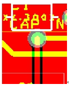
A via is a connection from one layer of the board to another. If you press “V” while you are routing, a via will be placed. After a via is placed you can route from the bottom or top layer, which ever suites you. In some instances the program will not allow you to place a via. In this case the place free via may be used. An example of a via is shown in below figure:
When you have a trace, and you do NOT want it to be unrouted during an autounroute, it is possible to lock the trace. To do this, simply click on the trace and press “L”, or right click and choose lock. This will prevent a trace from being changed at any time during the “Auto” functions.
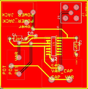
When you are routing through a copper pour, the pour will not repour until the screen is refreshed. After routing, the board will look similar to below Figure:
Make sure that every trace is checked by hand to make sure that all of the connections are made. It is possible to use the tool Auto → Design Rule Check to make sure that all of the connections are made. There will almost always be errors, however, you can check the errors and make sure that they are not important by clicking on the Error tool and then the Query tool, and click on an error. The error number and the error type can be seen in the Query window. The board design is now done, and it is now time to fabricate the board.


