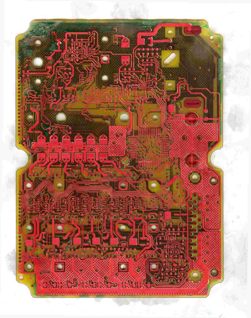
Reverse Engineering Printed Circuit Board Strategy
Reverse Engineering Printed Circuit Board Strategy will always refers to the component arrangement, since get the bill of material is very critical, in the bill of material, each one of the resistor, capacitor, inductor, crystal value, size and footprint must be measured and record, diode, triode and integrated circuit marking should be recorded properly too.
Reverse engineering circuit card’s documents means not only get its layout, and circuit pattern drawing, schematic diagram, but also its part list, which has the clear description about each components, so when in the process of component procurement for manufacture after reverse engineering, engineers can understand it well.

About the PRINTED CIRCUIT BOARD component location layout:
1, When redesign PCB component layout, engineer should make full use of legendary on the PRINTED CIRCUIT BOARD and mark each one of them on the layout, such as the frame marking for the attached bar code label, print a arrow on the PRINTED CIRCUIT BOARD to show the direction of wave soldering, use broken line to descript the outline of components on the bottom side which means the PCB board need only print one time legendary, etc.
2, draw the component reference marking and indicated instruction, and ensure all of these marks are all visible after components being inserted, these actions could be quite helpful, check and malfunction, it could be a very effective maintanence work;
3, the distance from the component to the board edge should be at least 1.5mm or 3mm at the best, which makes the PRINTED CIRCUIT BOARD become easier to be convey and wave soldering, and make the minimum damage to the external components;
Tags: reverse engineering circuit board,reverse engineering circuit card,reverse engineering pcb,reverse engineering pcb assemble,reverse engineering pcb board,reverse engineering pcb card,reverse engineering pcba,reverse engineering printed circuit board,reverse engineering printed wiring board,reverse engineering pwb,reverse engineering pwba

