Reverse Engineering PCB Board Schematic to avoid Power Supply Noise
Reverse Engineering PCB Board Schematic to decrease Power Supply Noise, extract printed circuit board wiring diagram from physical PCB board sample for a better performance;

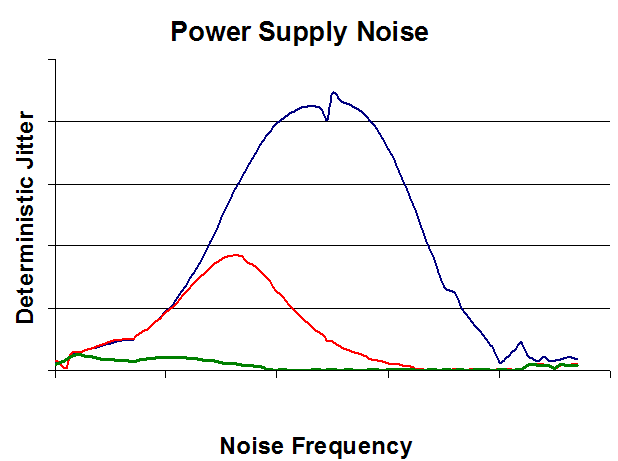
Common sources of interference in power supply circuitry diagram applications come from the power supply PCB source, and this interference signal is usually introduced through the power supply pins of active devices. For example, the timing diagram of the A/D converter output in below Figure. In this figure, the sampling speed of the A/D converter is 40ksps and 4096 samples are taken.

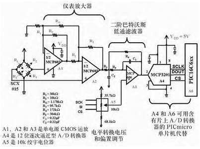
In this example, no bypass capacitors are added to the instrumentation amplifier, reference voltage source, and A/D converter. In addition, the input of the circuit is based on a low-noise, 2.5V DC voltage source.
In-depth study of the circuit shows that the noise source seen on the timing diagram comes from the switching power supply. Bypass capacitors and choke rings are added to the circuit. A 10µF capacitor is added to the power supply, and three 0.1µF capacitors are placed as close as possible to the power supply pins of the active components.
It can be seen on the generated new timing diagram that a stable DC output is produced. The histogram shown in Figure 3 can verify this. The data shows that these changes to the circuit eliminate the noise source from the circuit’s signal path.

