Reverse Engineering PCB Board Layout Design to Increase Heat Dissipation Efficiency
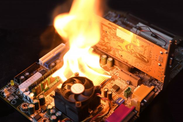
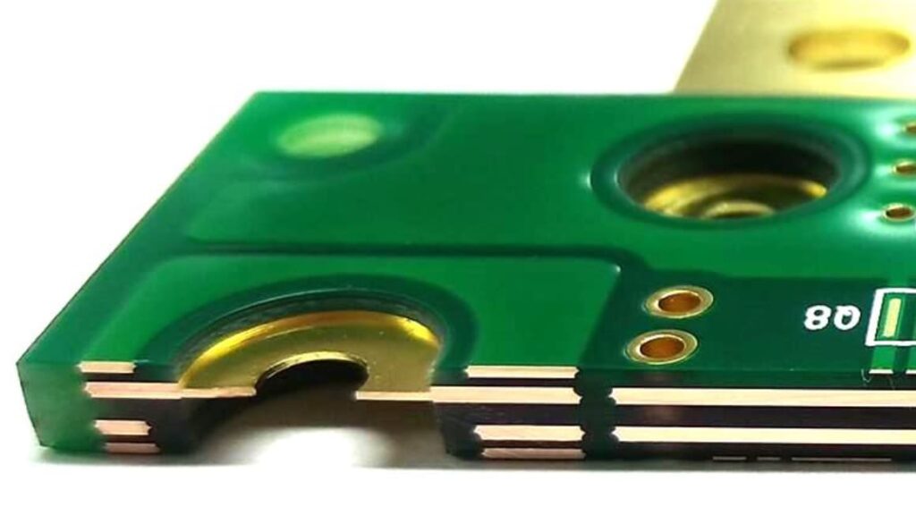
The currently widely used PCB boards are copper-clad/epoxy glass cloth substrates or phenolic resin glass cloth substrates, and a small amount of paper-based copper-clad boards are used. Although these substrates have excellent electrical properties and processing properties, they have poor heat dissipation. As a heat dissipation path for high-heating components, it is almost impossible to expect heat from the resin of the PCB itself to conduct heat, but to dissipate heat from the surface of the component to the surrounding air. However, through Reverse Engineering PCB Board Layout Design can effectively increase Heat Dissipation Efficiencyas.

Electronic products have entered the era of miniaturization so as printed circuit board, high-density mounting, and high-heating assembly, it is not enough to rely on the surface of a component with a very small surface area for heat dissipation while the heat dissipation for original PCB board design hasn’t been considered thoroughly.

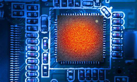
At the same time, due to the extensive use of surface mount components such as QFP and BGA, the heat generated by the components is transferred to the PCB board in a large amount. Therefore, the best way to solve the problem of heat dissipation is to improve the heat dissipation capacity of the PCB itself, which is in direct contact with the heating element, and conduct or radiate through the PCB board, reverse engineering PCB board layout design to make it with more space and efficiency for heat dissipation.


