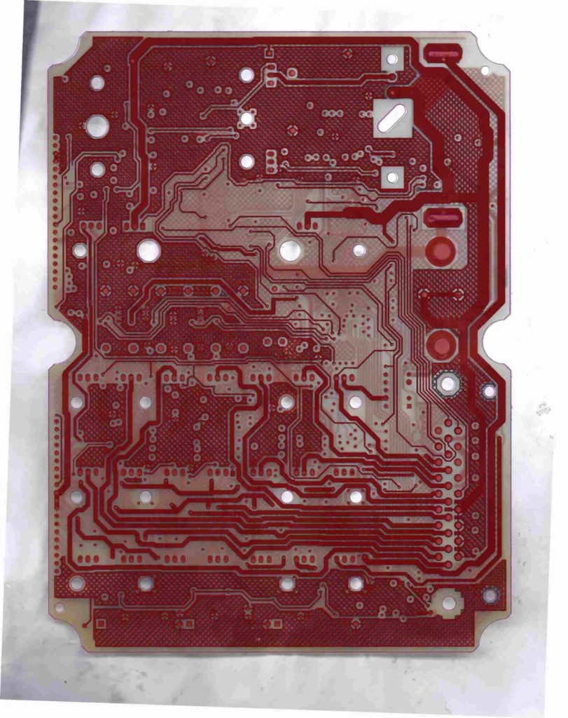
Reverse Engineering Electronic Circuit Board
Reverse engineering Electronic circuit board will always refers to the component arrangement, since get the bill of material from the process of reverse engineering printed wiring board is very critical, in the bill of material, each one of the resistor, capacitor, inductor, crystal value, size and footprint must be measured and record, diode, triode and integrated circuit marking should be recorded properly too.

Reverse PCB card means not only get its layout, and circuit pattern drawing, schematic diagram, but also its part list, which has the clear description about each component, so when in the process of component procurement for Electronic circuit board manufacture, engineers can understand it well.
Distribute the Cables and connectors on the Electronic circuit board:
1, don’t put the cable or wire onto the Electronic circuit card directly after file extraction, but use a connector, if the cables must connect to the Electronic circuit board directly, then there must be a terminal on the side of Electronic circuit board on the end of cables. Those cables which connects outside should be concentrated on the small area of Electronic circuit board which can makes them away from other components;
2, use cables with different colors when reverse engineering Electronic circuit board to avoid the mistakes emerge in the process of assemble. Each company has the unique color combination solution, for example, the cable with high electrical level use blue to represent them, then low electrical level use yellow, etc;
3, connectors should choose those with bigger pad size for better mechanical connection on them, the cables of connector with great amount of leads can makes easier to insert;
Tags: pcb assemble reverse engineering,pcb board reverse engineering,pcb card reverse engineering,pcb reverse engineering,pcba reverse engineering,Printed Circuit Board Reverse Engineering,printed wiring board reverse engineering,pwb reverse engineering,pwba reverse engineering

