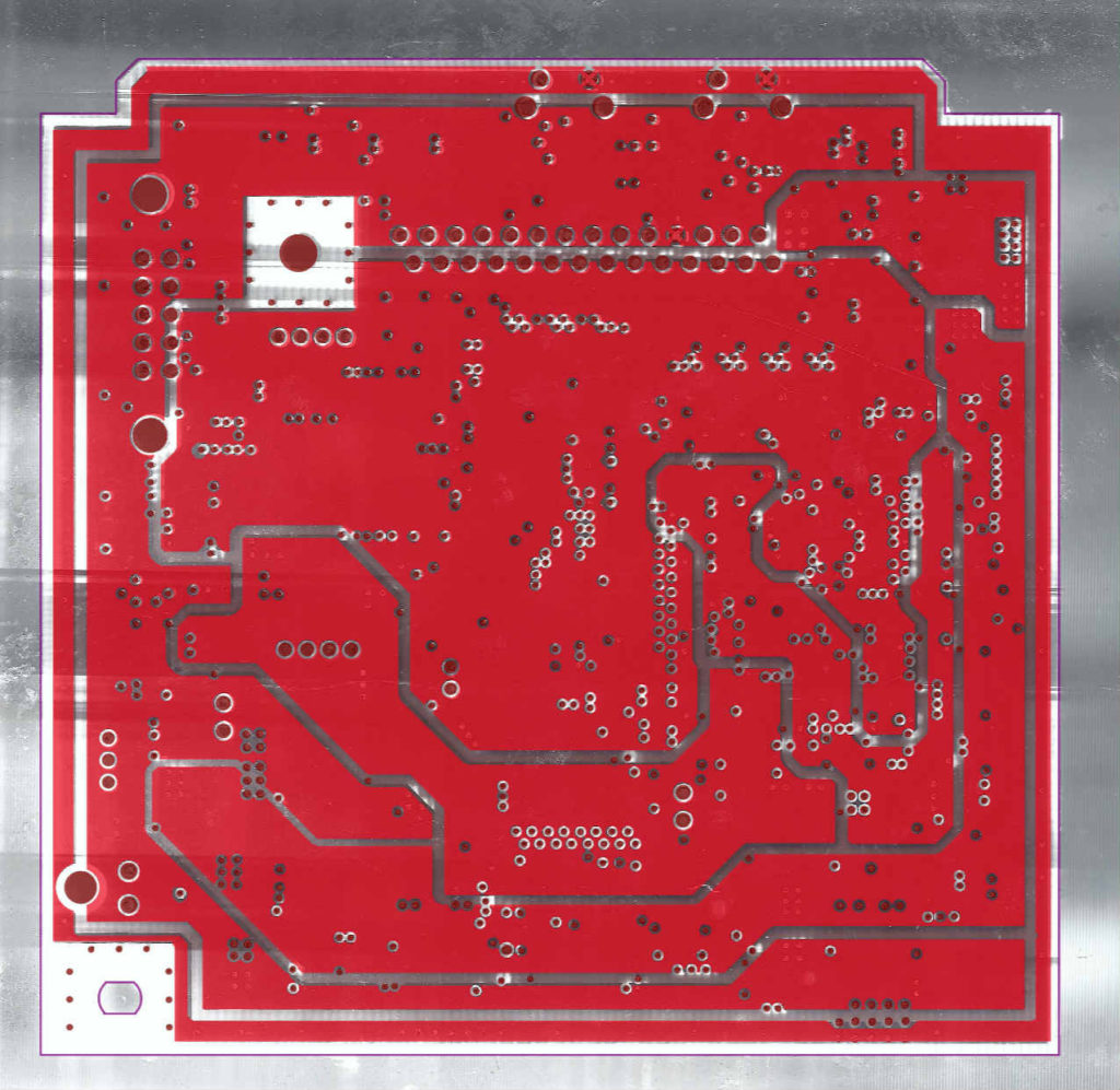
Reverse Engineering Circuit Board Gerber File
Reverse Engineering Circuit Board Gerber File will always refers to the component arrangement, since get the bill of material from the process of reverse engineering printed circuit board is very critical, in the bill of material, each one of the resistor, capacitor, inductor, crystal value, size and footprint must be measured and record, diode, triode and integrated circuit marking should be recorded properly too.

Reverse engineering PCB Board means not only get its layout, and circuit pattern drawing, schematic diagram, but also its part list, which has the clear description about each component, so when in the process of component procurement for Circuit Board manufacture, engineers can understand it well.
There might be some regular rules after this process done:
1, when cover the Circuit Board with coating, those areas without using coating should be identified on the drawing of engineering design. And the effect on the line among capacitors must be taken into consideration;
2, as for the through holes, in order to ensure the best performance of soldering on circuit board, the distance between lead and hole diameter must be at around 0.25mm to 0.70mm; through hole with larger size benefit the insertion when assemble circuit board reverse engineering, but if the engineer want to have a better capillary effect on the Circuit Board, there must be a balance between them;
3, should choose the pre-treat components according to the industry standard. Preparation of electronic components is one of the processes with lowest efficiency, except some extra procedures which can bring out the static charge damage risk and prolong the delivery time frame, it also increase the chance of making mistake;
4, specify the specification of most of the hand soldering components, and regulate the length of extra lead length no longer than 1.5mm than the surface of Circuit Board, which can decrease the time amount spend on component preparation and workload for lead recondition, and the Circuit Board can go through the wave soldering facility smoothly.
Tags: pcb assemble reverse engineering,pcb board reverse engineering,pcb card reverse engineering,pcb reverse engineering,pcba reverse engineering,Printed Circuit Board Reverse Engineering,printed wiring board reverse engineering,pwb reverse engineering,pwba reverse engineering

