Reverse Engineering a Multi-layer Printed Circuit Board
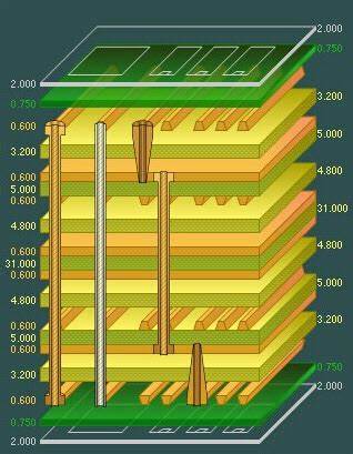
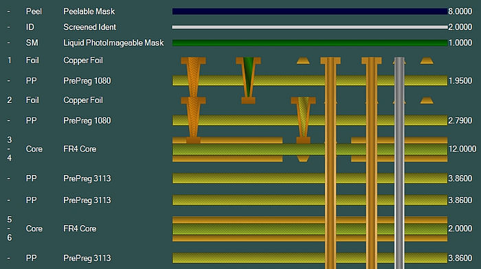
When Reverse Engineering a Multi-layer Printed Circuit Board, the layers should be designed symmetrical, and it is better to have an even number of copper layers. If it is asymmetrical, it is easy to cause distortion.

Multi-layer Printed Circuit Board wiring scheme layout redesign is carried out according to circuit functions. When relayout circuitry pattern on the outer layer, more wiring is required on the soldering surface and less wiring on the component surface, which is beneficial to the maintenance and troubleshooting of the printed board.
In terms of wiring, it is necessary to separate the power layer, ground layer and signal layer to reduce interference between power, ground, and signals. The lines of the two adjacent layers of printed circuit boards should be as perpendicular to each other as possible, or follow diagonal lines or curves, and not parallel lines to reduce the coupling and interference between the substrate layers.

The shape and size of the Multi-layer Printed Circuit Board must be based on the product structure. From the perspective of production technology, it should be as simple as possible. Generally, it should be a rectangle with a small aspect ratio to facilitate assembly, improve production efficiency and reduce labor costs. The number of layers must be determined according to the requirements of circuit performance, board size and circuit density.
For Multi-layer Printed Circuit Board, four-layer boards and six-layer boards are the most widely used. The layers of the multi-layer PC board should be symmetrical, and it is best to have an even number of copper layers, that is, four, six, eight, etc. Because of the asymmetric lamination, the board surface is prone to warping, especially for surface-mounted multilayer PCB boards, which should be paid more attention.

