

Reverse Design Double Side PCB Board Layout Manually
When Reverse Design Double Side PCB Board Layout Manually, in order to ensure the correct implementation of the circuitry pattern, some general printed circuit board design guidelines need to be followed: try to use the ground plane as the current loop;
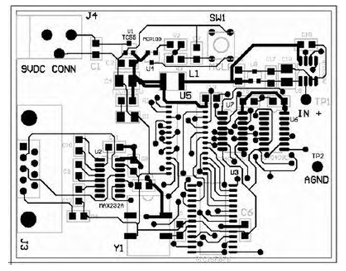
Separate the analog ground plane from the digital ground plane; if the ground plane is separated by signal traces, in order to reduce interference to the ground current loop, the signal trace should be perpendicular to the ground plane;
Place the analog circuit as close as possible to the edge of the circuit board, and place the digital circuit as close as possible to the power connection end. This can reduce the di/dt effect caused by the digital switch.
Both of these two types of double side PCB boards have a ground plane on the bottom layer when cloning gerber file. This approach is to facilitate engineers to solve problems and enable them to quickly understand the wiring pattern of the circuit board.
Manufacturer’s demonstration boards and evaluation boards usually use this double layer printed circuit board reverse engineering routing strategy. However, it is more common to place the ground plane on the top layer of the circuit board to reduce electromagnetic interference.