Restore Circuit Diagram From Existing Printed Wiring Board

Restore Circuit Diagram From Existing Printed Wiring Board

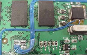
Restoring a circuit diagram from an existing Printed Wiring Board (PWB) is a crucial process in PCB reverse engineering. This involves extracting the schematic diagram either through PCB pattern files or by directly analyzing a physical electronic PCB sample. The primary purpose of this restoration process is to understand the working principles of the printed wiring board and its functional environment. Additionally, a circuit diagram obtained from PCB restoration can be instrumental in analyzing the functional features of an electronic product.

Importance of PCB Circuit Diagram Restoration

Restoring a circuit diagram is an essential step in both PCB reverse engineering and electronic product analysis. It serves multiple purposes, including the examination of a PCB board’s working principle, troubleshooting, and the development of improved or modified designs. Whether used for repairing existing devices or as a foundation for new printed circuit board designs, a restored wiring diagram provides critical technical insights.

Mevcut bir Baskılı Kablolama Kartından (PWB) bir devre şemasını geri yüklemek, PCB tersine mühendisliğinde önemli bir işlemdir. Bu, şematik diyagramı PCB desen dosyaları aracılığıyla veya doğrudan fiziksel bir elektronik PCB örneğini analiz ederek çıkarmayı içerir. Bu geri yükleme işleminin birincil amacı, baskılı kablolama kartının çalışma prensiplerini ve işlevsel ortamını anlamaktır. Ek olarak, PCB geri yüklemesinden elde edilen bir devre şeması, bir elektronik ürünün işlevsel özelliklerini analiz etmede etkili olabilir.

For engineers engaged in PCB design after reverse engineering, a restored circuit diagram acts as a reference that facilitates accurate layout reproduction, component placement, and signal path verification. This process is particularly valuable in industries where legacy electronic circuit boards require duplication, modification, or functional improvement.

Восстановление принципиальной схемы из существующей печатной платы (PWB) является важнейшим процессом в обратном проектировании печатных плат. Это включает в себя извлечение принципиальной схемы либо через файлы шаблонов печатных плат, либо путем прямого анализа физического образца электронной печатной платы. Основная цель этого процесса восстановления — понять принципы работы печатной платы и ее функциональной среды. Кроме того, принципиальная схема, полученная в результате восстановления печатной платы, может быть полезна для анализа функциональных особенностей электронного продукта.

Applications of Restored PCB Circuit Diagrams

A circuit diagram derived from PCB restoration plays a significant role in various aspects of product development and maintenance. These include:

  1. Reverse Engineering & Functional Analysis – By restoring a circuit diagram, engineers can better understand how an electronic product operates, enabling enhancements, replication, or redesign.
  2. PCB Design Support – The restored diagram serves as a blueprint for further modifications and improvements, ensuring compatibility with existing systems.
  3. Product Adjustment & Optimization – Engineers can refine product performance by analyzing and modifying specific circuit elements.
  4. Repair & Troubleshooting – Faulty electronic devices can be diagnosed and repaired more efficiently with an accurate schematic diagram.
  5. Modification & Upgrades – Older PCB boards can be modernized by integrating new components while retaining their original functionality.

Our Professional PCB Restoration Services

Przywracanie schematu obwodu z istniejącej płytki drukowanej (PWB) jest kluczowym procesem w inżynierii wstecznej PCB. Obejmuje to wyodrębnienie schematu albo za pomocą plików wzorów PCB, albo poprzez bezpośrednią analizę fizycznej próbki elektronicznej PCB. Głównym celem tego procesu przywracania jest zrozumienie zasad działania płytki drukowanej i jej środowiska funkcjonalnego. Ponadto schemat obwodu uzyskany z przywracania PCB może być pomocny w analizie cech funkcjonalnych produktu elektronicznego.

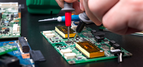
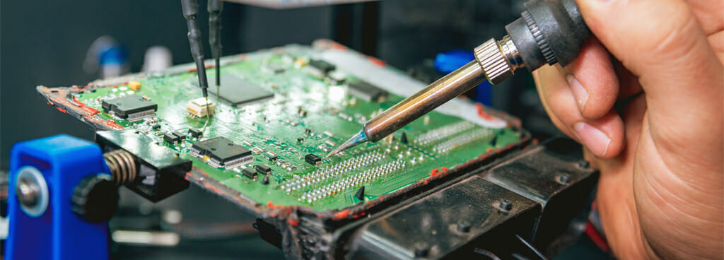
Restoring PCB circuit diagrams is a critical part of our service catalog. Whether you need to replicate, modify, or analyze a PCB board, we can deliver 100% accurate circuit diagrams. Simply provide us with a sample PCB prototype or a PCB layout file, and our team will extract and reconstruct the schematic with precision.


Tags: ,,