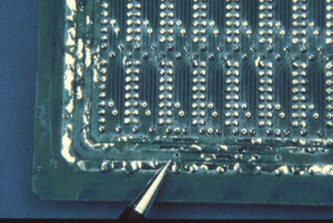
Printed Wiring Board Clone Defects
Printed Wiring Board Clone Defects can be caused by several reasons, hereby we would like to introduce several reasons:
The solderability of printed wiring board hole will affect the PCB cloning quality, if the holes don’t have a good solderability, cold soldering will occur and affect the component parameter in the printed wiring board, especially for multilayer pcb board cloning will cause component and internal layer unreliability which will ultimately cause the malfunctioning of whole system.
Solderability means the features of metallic surface after the solder tin melted down, and form a relative even, constant and smooth adhesive thin film on the surface. There are several items will affect the solderability:
1 component of solder tine and features of printed wiring board pad; solder tin is the most important ingredient of chemical processing, which was constituted by chemical ingredient containing flux. The most usual low melt down metal is SN-PB or SN-PB-AG.
2 soldering temperature and metal plate surface cleanness will also affect the process. If overheated, then the solder tin spreading speed will be faster and higher flexibility, which will cause the printed wiring board and solder tin surface oxidated immediately and bring the defect. If the surface of printed wiring board being contaminated will also caused the inferior assembly quality include solder tin ball and drop, open circuit and etc.
Tags: pcb assemble clone,pcb board clone,pcb card clone,pcb clone,pcba clone,printed circuit board clone,printed wiring board clone,pwb clone,pwba clone


