Printed Circuit Board Layout Cloning
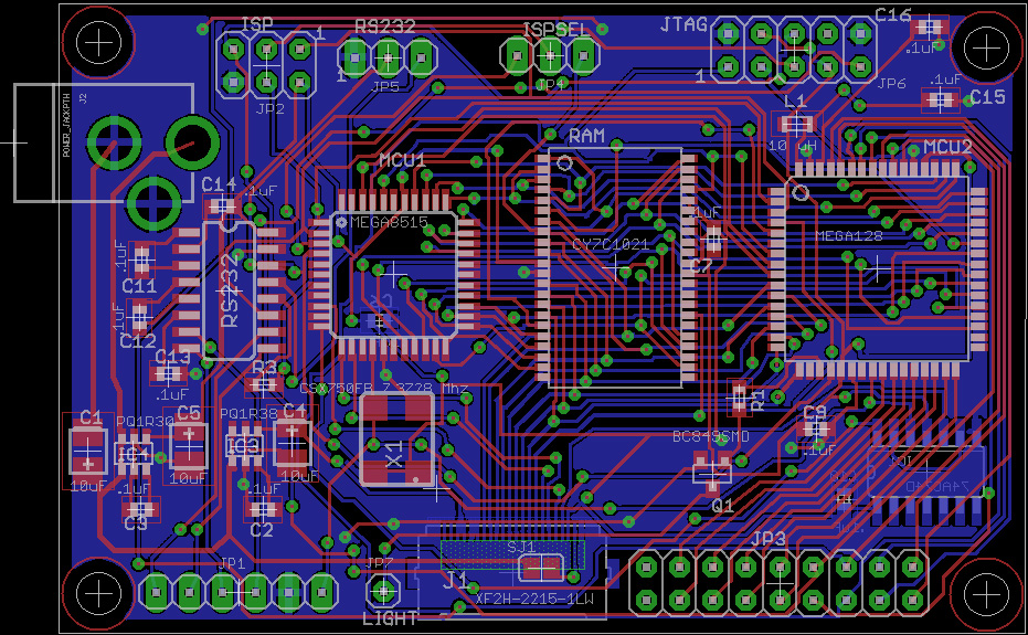
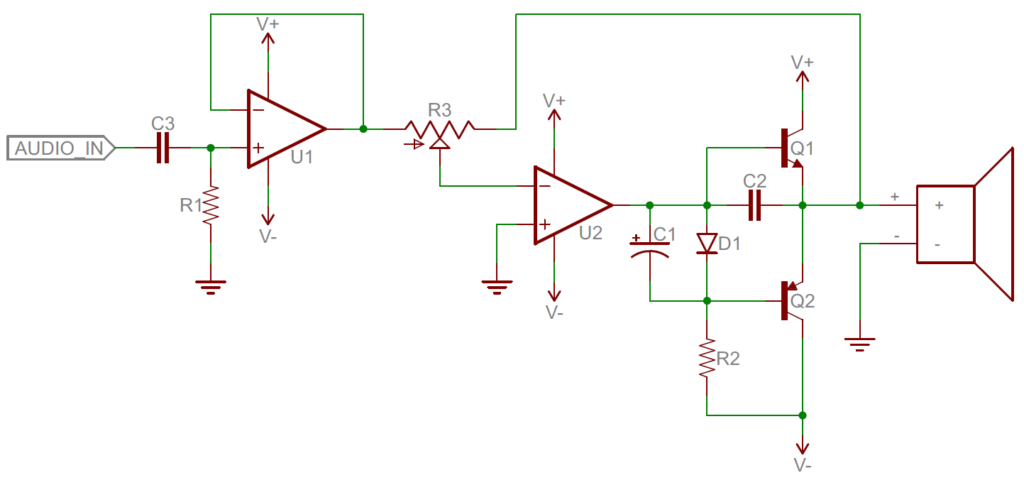
Printed Circuit Board Layout Cloning is a process to place electronic components on the PCB board design drawing which has been created through schematic diagram, the re-layout is to put electronic components on the circuit board. At this time, if all the preparations mentioned above are done, you can generate it on the schematic Netlist (Design->Create Netlist), and then import the netlist (Design->Load Nets) on the PCB diagram.

Just saw The devices are all piled up, and there are flying wires between the pins to indicate the connection. Then you can re-layout printed wiring board design. General layout press need to be proceeded with the following principles:
1. According to the reasonable division of electrical performance, it is generally divided into: digital circuit area (that is, afraid of interference and interference), analog circuit area (fear of interference), power drive area (interference source);

2. Circuits that complete the same function should be placed as close as possible, and the components should be adjusted to ensure the most concise connection; at the same time, adjust the relative position between the functional blocks to make the connection;
3. For high-quality components, the installation location and installation strength should be considered; heating components should be placed separately from temperature-sensitive components, and heat convection measures should be considered when necessary;

