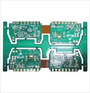
Printed Circuit Board Introduction
1, General introduction of Printed Circuit Board
Printed circuit board is important component in the electronic product, is the carrier of electronic components and electricity connection provider. Traditional printed circuit board use printed etching and solder resistance method to produce the circuitry pattern which comes its name. due to the increasing minimization and finest, most of the printed circuit boards are applying the adhesive etching resistance and after exposure/development to produce printed circuit board.
2, Printed circuit board structure:
Printed circuit board is composited by soldering pad, through hole, fixed hole, tracks, components, inserting parts, filling area, edge, etc. the most commonly seen layer structure includes SINGLE LAYER PCB, DOUBLE LAYERS PCB and MULTILAYER PCB.
The main functions of each composed parts:
Soldering pad: use for soldering the pins on the components;
Through hole: with metal through hole and un-metal through hole, the metal through hole is used for electrical connection among different layers;
Fixed hole: use to install printed circuit board;
Lead: the electrical network copper foil among the components;
Insert part: provide the connection among different printed circuit boards;
Filling: use the copper foil to fill the groundling network to effectively reduce the resistance;
Electrical edge: it can be used to determine the dimension of printed circuit board, and all of the components on it can’t over the edge;


