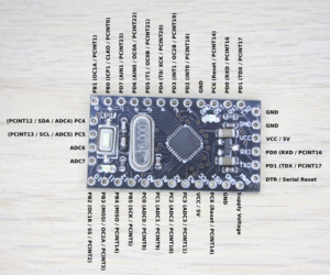
Pin Arrangement in PCB Board Reverse Engineering
Pin Arrangement in PCB Board Reverse Engineering
The task of SMT assembly drawing in placement through PCB Board Reverse Engineering is to position all components on the PCB board in a way that is feasible with respect to the limitations of the production process. After that all nets, i. e., all connections between the pins of the components according to the logical design, have to be routed on the PCB.
Obviously, the placement has tremendous repercussions on the routing. Since the conditions on the placement itself are usually relatively simple, e. g., components are not allowed to overlap and have to adhere to some minimum distances, the main objective in placement is to allow a good and feasible routing.
In principle it would be best to perform placement and routing in one step. But due to the difficulties involved, both tasks are typically done sequentially in practice.
As said above, since finding a physically feasible placement is generally easy, the main objective of the placement is to permit a high quality routing. However, it is difficult to define “high quality” in a somewhat precise mathematical sense. Instead, substitute objectives are defined. A widely used objective in practice is to minimize the total wire length of all connections.
Unfortunately, the exact wire length of each net is not known until the nets are actually routed. Since even the computation of the minimum length of a single net is in general NP -hard, as it corresponds to computing the length of a minimum Steiner tree, the total wire length has to be estimated.
This is usually done by summing up an estimate of the length of each individual net. Methods to estimate the length of a specific net include: heuristically computing a Steiner tree between the terminals, computing a minimum spanning tree between the terminals, building a chain through the terminals, or taking half the length of the perimeter of the bounding box enclosing all the terminals of the net.
Keep in mind, that for nets with two terminals and using Manhattan distances (a typical metric of VLSI design) all these measures give the same result.


