PCB Reverse Engineering Introduction

PCB Reverse Engineering, also known as PCB Clone or PCB Copy, is using Reverse Engineering technology onto the PCB which was designed and manufactured by others, it is to use PCB Board related software to copy someone else’s Printed Circuit Board and then manufacture the PCB Circuit Board by yourself.
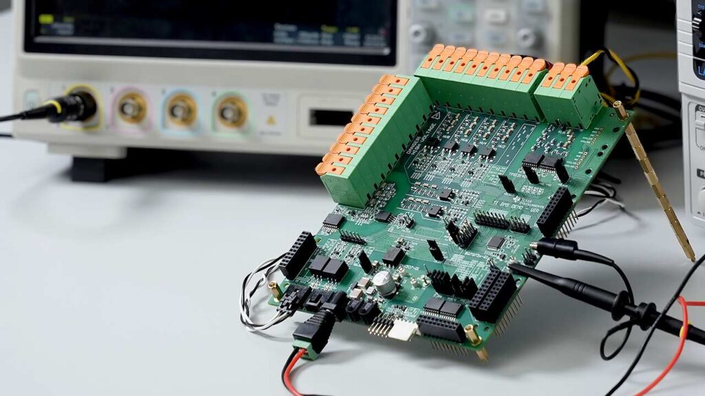
PCB 역엔지니어링은 단순히 보드를 복사하는 것 이상입니다. 조직이 기존 전자 제품을 복원, 복제, 심지어 향상시킬 수 있도록 하는 복잡하고 고도로 기술적인 분야입니다. 손실된 설계를 복제하거나, 귀중한 레이아웃 데이터를 복구하거나, 혁신을 위해 역엔지니어링하려는 경우 이 프로세스는 현대 전자 제품 수명 주기 관리에서 중요한 역할을 합니다. 회로도, Gerber 파일, 넷리스트 및 레이아웃 도면을 정확하게 추출하여 회사는 오늘날 빠르게 변화하는 기술 환경에서 연속성, 규정 준수 및 경쟁력을 보장할 수 있습니다.

PCB Reverse Engineering is a specialized technical process used to analyze and reconstruct an existing Printed Circuit Board (PCB) when the original design data is unavailable or lost. This process involves various techniques to recover, restore, or recreate the schematic diagram, layout drawing, Gerber files, and other essential data files needed for the reproduction or remanufacture of the board. PCB reverse engineering serves as a valuable solution for redesign, product improvement, repair, or even legacy system support.
A Engenharia Reversa de PCB é um processo técnico especializado usado para analisar e reconstruir uma Placa de Circuito Impresso (PCB) existente quando os dados do projeto original não estão disponíveis ou são perdidos. Este processo envolve várias técnicas para recuperar, restaurar ou recriar o diagrama esquemático, desenho de layout, arquivos Gerber e outros arquivos de dados essenciais necessários para a reprodução ou remanufatura da placa. A engenharia reversa de PCB serve como uma solução valiosa para redesenho, melhoria de produto, reparo ou até mesmo suporte a sistemas legados.

This is the traditional explanation for the PCB Reverse Engineering. with the technology development, the impact and scope of this industry continues to expand rapidly, and the definition of PCB Reverse Engineering also extend from the narrow sense that it only refers to extraction of Printed Circuits Boards files from electronic Circuit Board and then restore it for the purpose of PCB Duplicate or PCB Replicate;

To the wide sense that PCB Reverse Engineering not only include PCB Restoration, PCB Clone and PCB Copy and other related technical aspect, but also modify Printed Circuit Board file, the shape of the mold for electronic products, extraction of 3-dimensional model data on a variet of electronic products, compile the components list assembled on the Printed Circuit Board as well as individual data sheets on each component where available, decrypt microcontroller on the Electronic PCB, crack MCU on the PCB Board, moreover, disassemble the firmware extracted from Microcontroller which include the content from both eeprom and flash, a whole set of PCB Reverse Engineering technology.
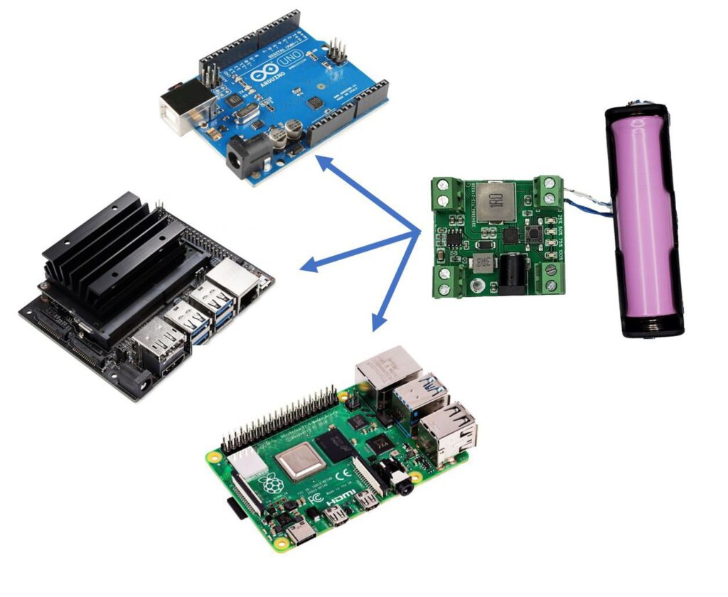
Обратный инжиниринг печатных плат — это специализированный технический процесс, используемый для анализа и реконструкции существующей печатной платы (ПП), когда исходные данные о проекте недоступны или утеряны. Этот процесс включает в себя различные методы восстановления, реставрации или воссоздания принципиальной схемы, чертежа компоновки, файлов Gerber и других важных файлов данных, необходимых для воспроизведения или повторного производства платы. Обратный инжиниринг печатных плат служит ценным решением для перепроектирования, улучшения продукта, ремонта или даже поддержки устаревших систем.

Circuit Engineering Company Limited provide a complete PCB Reverse Engineering service, Rapid Prototyping and functional test services using the latest technologies combined with traditional skills for a wide range of industries. By integrating our traditional skills with the latest technologies, we can offer clients a comprehensive portfolio of product development services all under one roof. For more details please contact our customer service team.


Tags: ,,,,,