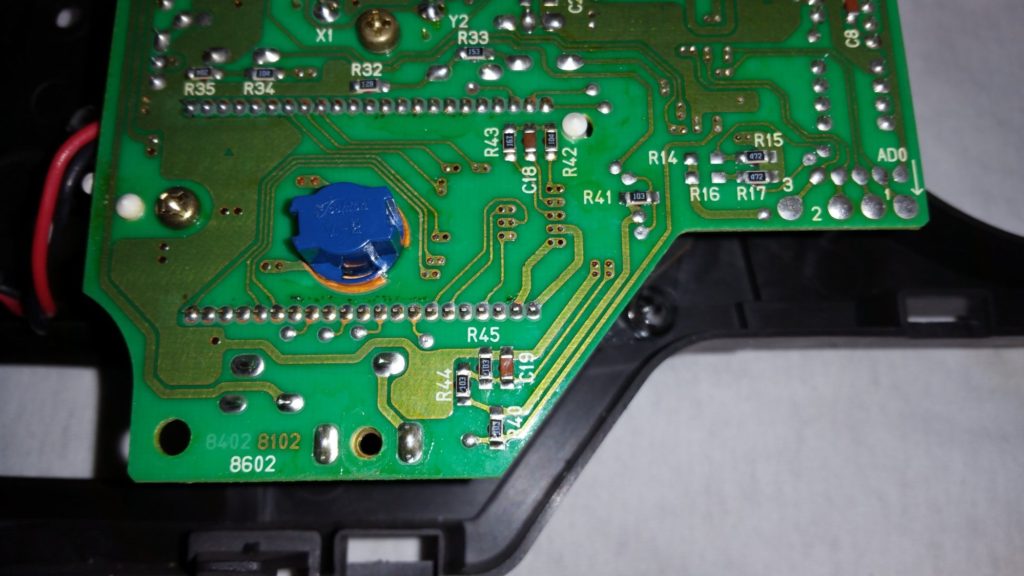
PCB Circuit Board Reverse Engineering Grounding Point
PCB Circuit Board Reverse Engineering Grounding Point is an critical point in the layout design file which will greatly affect the performance of PCB circuit board functionality;

In the process of Pcb circuit board Reverse Engineering, the grounding point on the same circuit level should be as close as possible, and power supply wave filtering capacitor from same level after high speed printed circuit board reverse engineering should be placed on this point. Especially for the transistor base anode, and the transmitting polar shouldn’t be too far away from each other, otherwise will cause interference and self-activation due to the extremely long distance of copper foil;
1, there is no cross line in the PCB board schematic diagram, as for the tracks on the pcb circuit board which could probably have the crossing scenario, designer should use “drill” or “bypass” methods to solve it, which means the able to cross track to go through the gap among other resistors, capacitors or triode, or bypass a terminal of one lead which could possibly cross, in the special condition if the circuit diagram is very complicate, crossing line is allowable in order to simply the design and solve the crossing track issue;
2, as for the resistor, diode and tube inductor, they have two assemble ways: one is the vertical another is horizontal, horizontal means the parts can vertically assemble on the Pcb circuit board, the advantage of this method is the space saving, horizontal type means the assemble occurs on the Pcb circuit board parallel, the advantage of this method is the mechanical strength of the part on the reverse engineering PCB is better. As for these two different assemble methods, the tooling holes pitch on the Pcb circuit board is different;
Tags: pcb assemble replicating,pcb board replicating,pcb card replicating,pcb replicating,pcba replicating,printed circuit board replicating,printed wiring board replicating,pwb replicating,pwba replicating

