PCB Board Reverse Engineering Procedures
PCB Board Reverse Engineering Procedures starts from
1. Determine the number of layers
The number of signal layers is determined according to the signal lines with special requirements, such as differential lines and sensitive signal lines, and the inner electrical layer (internal power supply and ground layer) is determined according to the type of power supply, isolation and anti-interference requirements. Layout count of a printed circuit board has greatly determined the first yielding rate, overall cost, time frame and complexity level of reverse engineering electronic circuit board;

2. The order of placement of circuits on each layer
One is the distribution of the special signal layer, and the other is the distribution of the power supply layer and the ground layer. The signal layer is adjacent to the internal electrical layer; the internal power supply layer and the ground layer are closely coupled and adjacent; the high-speed signal transmission layer of the circuit is in the signal intermediate layer, that is, between the two internal electrical layers, shielding; To avoid two signal layers adjacent; A signal The layer and the B signal layer are connected to their own separate ground planes to reduce common mode interference.

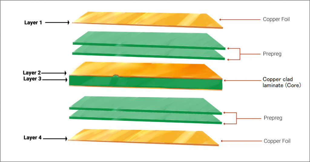
3. Four-layer board, six-layer board stacking method
The four-layer board is from top to bottom: signal 1—gnd—power—signal 2;
The six-layer board is from top to bottom: signal 1—gnd—signal 2—power—gnd—signal 3;

