PCB Board Low Inductance Grounding System Application
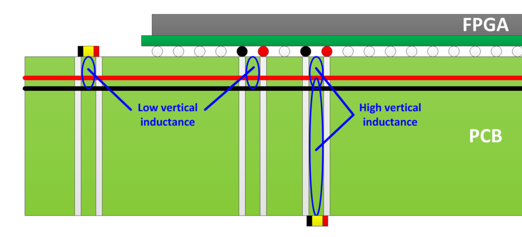
PCB Board Low-inductance grounding systems are the most important factor in minimizing EMC problems through PC Board reverse engineering. Maximizing the grounding area on the PCB circuit board can reduce the system grounding inductance, thereby reducing electromagnetic radiation and crosstalk.

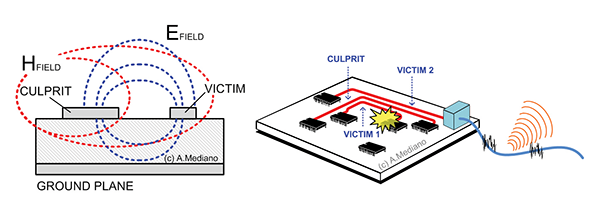
Crosstalk can exist between any two wires on the circuit board which can be prevented by reverse engineering PCB board, depending on the mutual inductance and mutual capacitance, and is proportional to the distance between the wires, the edge rate, and the wiring impedance.

In high speed digital signal PCB board systems, the crosstalk generated by mutual inductance is usually greater than the crosstalk generated by mutual capacitance. Mutual inductance can be reduced by increasing the spacing between wiring or reducing the distance to the ground plane in the PCB board layout.

