Multilayer Printed Circuit Board Reverse Engineering
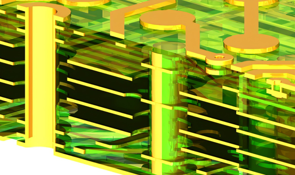
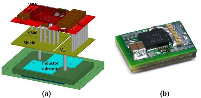
Multilayer Printed Circuit Board Reverse Engineering means each one of the layers among the multilayer PCB board need to be copied and draw its layout accordingly, and there is pre-design and reliable interconnection among them.

All the drill and plating has been done when all these layers circuitry pattern being drawn, the technology of multilayer printed circuit board reverse engineering disobey the traditional processing procedure from the starting point and the most internal layers are formed by a double layer printed circuit board. while the outside layers are made by individual copper foil layer.

Before lamination, internal layer must be drilled, plating pattern and image transfer, exposure and etching. The outer layer being drilled is the signal layer of multilayer printed circuit board, it manipulate the electrical connection through inner rim edge to form an even copper ring. Follow by multilayer printed circuit board reverse engineering press from various layers and can assembly the component through wave-flow.

Multilayer printed circuit board reverse engineering being applied in the field of professional electronic device like computer and military device, especially when over-size and over-weight, however it can only use the higher cost of multilayer PCB Board for more space and lighter weight. In the high speed circuit, it is quite useful since it can let the designer has more space for layout and larger area for grounding and power supply area.
Tags: pcb assemble reverse engineering,pcb board reverse engineering,pcb card reverse engineering,pcb reverse engineering,pcba reverse engineering,Printed Circuit Board Reverse Engineering,printed wiring board reverse engineering,pwb reverse engineering,pwba reverse engineering

