Low DC Impedance PCB Board Layout
Low DC Impedance PCB Board Layout at the Point of Load
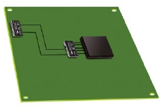
Ideal PCB Board layout of copper planes at the point of load is dependent upon the type of loading being applied. There are essentially two types of high-current, low-voltage load configurations: a) single device high current load (Fig. 1)
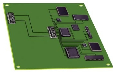
and b) multiple devices powered by a single low-voltage rail. (Fig. 2).
For typical low-voltage, high-current applications DC impedance and AC impedance (inductance) must be minimized. Minimizing DC impedance in a PCB Board layout requires an analysis using squares to determine the geometry and the impedance of the interconnect.
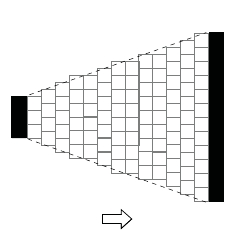
A square of 1 oz.copper will have a resistance of 0.641 mΩ between parallel edges, regardless of square dimension (Fig. 3).
It is important to note that the current must originate and flow evenly from edge to edge of the square. If the geometry of the source or load is such that current would not flow evenly from edge to edge of the square, the square geometry must be reduced in size (Fig. 4).


