Layout PCB Board Signal Line
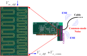
When engineer layout PCB Board Signal Line, A filter capacitor is placed at the connector or within 25 mm of the receiving circuit.
(1) Connect to the chassis ground or receive circuit ground with a short and thick wire (length less than 5 times width, preferably less than 3 times width).
(2) The signal line and the ground line are first connected to the capacitor and then connected to the receiving circuit.

Layout PCB Board Signal Line
Make sure the PCB board signal line is as short as possible when layout it
When the length of the signal line is greater than 300mm, it is necessary to layout a ground wire in parallel. Make sure that the loop area between the signal line and the corresponding loop is as small as possible. For every few centimeters of the long signal line, the position of the signal line and the ground line should be changed to reduce the loop area.
Driving signals from a central location of the network into multiple receiving circuits. Make sure that the loop area between the power supply and ground is as small as possible, placing a high frequency capacitor close to each power supply pin of the integrated circuit chip.
Driving signals from a central location of the network into multiple receiving circuits, where possible, the unused areas are filled with ground and the fill areas of all layers are connected every 60 mm. Make sure to connect to ground at two opposite end positions of any large ground fill area (approximately greater than 25mm x 6mm).
When the length of the opening on the power supply or ground plane exceeds 8 mm, connect the two sides of the opening with a narrow wire. The reset line, interrupt signal line, or edge trigger signal line cannot be placed near the edge of the PCB.


