Layout Copper Pour on PCB Reverse Engineering File
Layout Copper Pour on PCB Reverse Engineering File
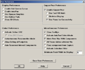
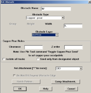
A copper pour is put on the bottom layer of the PCB board, and will act as a ground plane. To set up for a copper pour click on Options → User Preferences. The following window as seen in below Figure will appear.Make sure that the “Enable Copper Pour”, and the “Use Pours for Connectivity” boxes are checked. Now it is time to make the pour. Click on the Obstacle tool from the toolbar, and right-click to select a new obstacle. Then right-click and select Properties. Change the values to what is shown in below Figure.
Make sure that the “Net Attachment” is chosen to link the ground net. Click “OK” and draw your pour with the same dimensions overtop of the board outline of PCB Reverse Engineering. You will see the board go red. If it goes green, you have chosen the top layer instead of the bottom layer. The board should now look something like below Figure.
You will see that the ground nets on all of the through-hole components disappear. These grounds will be connected directly to your ground plane through a thermal relief. Click on Options → Thermal Relief Settings, and change your small thermal relief spoke width to 20 mils. Click Auto → Refresh All, and the width of the spokes of your thermal relief should have changed to 20 mils from default 10 mils. We do this so that you do not have problems in the etching phase from PCB Reverse Engineering.
Note: Auto → Refresh all will be used often in the remainder of this tutorial, and I will refer to it as “refreshing the board”.


