Inverter PCB Board of Electrical Vehicle Schematic Diagram Cloning
In the rapidly evolving electric vehicle (EV) industry, the demand for efficient and reliable power conversion systems is paramount. At the heart of these systems lies the electrical vehicle inverter PCB board, a critical component responsible for converting direct current (DC) from the battery into alternating current (AC) to drive the motor. Our specialized services focus on providing comprehensive solutions for Electrical Vehicle Inverter PCB Board Schematic Diagram Cloning, offering clients the ability to replicate, duplicate, and restore these essential boards with precision and expertise.
Our core service revolves around reverse engineering EV inverter PCB boards to generate accurate schematic diagrams, BOM lists, netlists, and CAD files (Travis, 2023). This enables us to reproduce the original design, create Gerber files, and develop pick & place data for efficient PCB assembly (asahoglund, 2023). Whether you need to copy a design, modify an existing board, remanufacture an obsolete component, or create a functional prototype, our team has the skills and technology to deliver high-quality results.
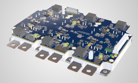
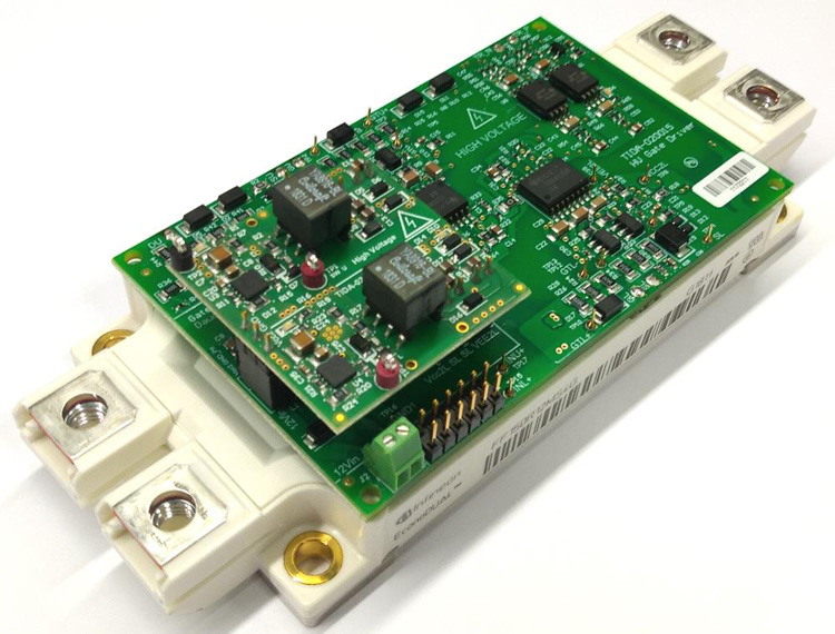
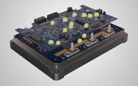
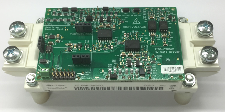
EV inverter PCBs possess unique features that distinguish them from boards used in other applications. They are designed to handle high power densities (PCBs for New Energy Vehicle, n.d.), manage significant heat dissipation, and operate under demanding automotive conditions (asahoglund, 2022). The components used, such as high-speed switching devices like Insulated Gate Bipolar Transistors (IGBTs) or Silicon Carbide (SiC) transistors, capacitors, and resistors, are carefully selected for their performance and reliability in high-voltage and high-current applications (The Vital Roles of EV Powertrain Components – Exro Technologies, 2024). The circuitry design emphasizes efficient power transfer, minimal electromagnetic interference (EMI), and robust protection mechanisms (The Ultimate Guide to Inverter PCBs: Design, Function, and Selection, 2025).
Reverse engineering EV inverter PCBs presents several challenges. The complexity of multilayer boards, the miniaturization of components, and the presence of proprietary designs can make the process intricate and time-consuming. Accurately identifying components, mapping out circuit connections, and understanding the board’s functionality require experienced engineers and specialized equipment. Additionally, high voltage can create damages over time, when the PCB itself has traces with voltages above 500V. Our team’s expertise in PCB design, coupled with our advanced reverse engineering techniques, allows us to overcome these difficulties and deliver accurate and reliable results. We utilize both manual and automated methods, including X-ray tomography and delayering, to ensure a comprehensive understanding of the board’s structure and function.
By choosing our services, clients gain access to a wealth of knowledge and experience in electrical vehicle inverter PCB board schematic diagram cloning. We provide tailored solutions to meet your specific needs, whether it’s replicating a legacy design, optimizing an existing product, or developing a new EV power conversion syste. Our commitment to quality, precision, and customer satisfaction makes us the ideal partner for all your EV inverter PCB board requirements.