

How to design Microstrip Transmission Lines in PC Board Replicating
How to design Microstrip Transmission Lines in PC Board Replicating
When design Microstrip Transmission Lines in PC Board Replicating process, for a simple two-sided PCB design where one side is a ground plane, a signal trace on the other side can be designed for controlled impedance. This geometry is known as a surface microstrip, or more simply, microstrip.
A cross-sectional view of a two-layer PCB illustrates this microstrip geometry as shown in below Figure.
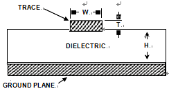
A Microstrip Transmission Line with Defined Impedance
For a given PCB laminate and copper weight, note that all parameters will be predetermined except for W, the width of the signal trace. Equation 1 can then be used to design a PCB trace to match the impedance required by PC Board replicating. For the signal trace of width W and thickness T, separated by distance H from a ground (or power) plane by a PCB dielectric with dielectric constant εr, the characteristic impedance is:


As an example including these calculations, a 2-layer board might use 20-mil wide (W), 1 ounce (T = 1.4) copper traces separated by 10-mil (H) FR-4 (ε = 4.0) dielectric material. The resulting impedance for this microstrip would be about 50 Ω. For other standard impedances, for example the 75 video standard, adjust “W” to about 8.3 mils.