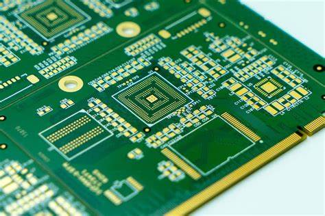
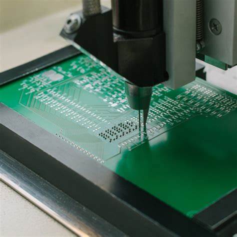
High Density Circuit Board Gerber File Cloning
High Density Circuit Board Gerber File Cloning is increasingly challenged by several factors:
physical sample: normally the target for HDI PCB board reverse engineering is difficult to acquire;
finer pitch pin spacing, because high density PCB board needs to layout the great amount of parts on circuitry pattern with limited space;
In-surfficient financial support, reverse engineering high density PCB normally require quite a few of money and time, mounting must be very precise, and the environment limitation.
Many plastic packages absorb moisture, causing the crack on assembly processing. Physical factors also include the complexity of the installation process and the reliability of the final product. Further financial decisions must consider how the PCB board will be manufactured and assembled.
More fragile pin components, such as SQFP, shrink quad flat packs with 0.50 and 0.40mm?0.020” and 0.016” pin pitches, may be it will present a challenge to an assembly specialist in maintaining consistent assembly process qualification rate.

The most successful re-development plans are the high density PCB board design guidelines and pad geometries that have already undergone process certification.
In terms of environment, the pad geometries may be different and it is based on the type of welding used to mount the electronic parts. When it becomes possible, the pad shape should be defined in a way that is transparent to the mounting process used.
Whether the parts are mounted on one or both sides of the PCB board, subjected to wave soldering, reflow soldering, or other methods, the pad and part dimensions should be optimized to ensure proper solder joints and inspection criteria.

Although the soldering patterns are dimensionally defined, and because it is part of geometry shape of printed circuit board, they are limited by the level of producibility and the tolerances associated with plating, corrosion, assembly, or other conditions.
The productivity aspect is also related to the use of the solder mask and the alignment of the solder mask to the conductor pattern.

