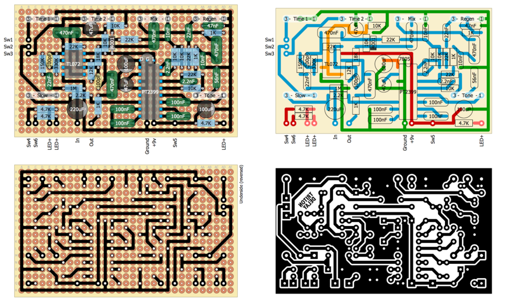
Electronic PCB Board Cloning Notes
There are Electronic PCB Board Cloning Notes must be set and follow when restore PCB board layout, gerber file and schematic out from physical target:

The bottom side of Electronic PCB Board is the grounding layer which provide the shielding layer and reference plane for the top layer which can provide great effect on the PWB reverse engineering emc result;
1 Keep on avoiding the adjacent signal layers neighbor to one another;
2 The main power supply should neighbor with the corresponding ground layers;
3 pay attention to the paired lay-up structure;
As for the mother board layer arrangement, it is difficult to control the parallel layout with long distance on it. as for those boards with working frequency higher than 50Mhz, please follow the below suggestion:
Component side and soldering side should be the complete ground plane for the purpose of shielding;
No parallel adjacent layout layer;
All of the signals layer should neighbor with the ground layer;
Critical signal should neighbor with ground layer without any physical separation;
Electronic PCB Board Cloning is a process that can be used by manufacturing companies to create digital inventories of spare parts or to convert legacy data into today’s CAD environments. It turns out that PCB reverse engineering methods are as much a key to the future of electronic PCB card manufacturing as CAD has been.
Tags: pcb assemble cloning,pcb board cloning,pcb card cloning,pcb cloning,pcba cloning,printed circuit board cloning,printed wiring board cloning,pwb cloning,pwba cloning

