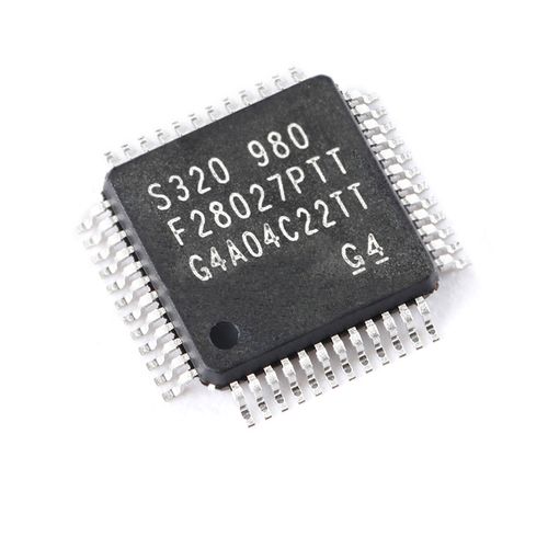
DSP Microprocessor TMS320F28027 Flash Program Replication
DSP Microprocessor TMS320F28027 Flash Program Replication will help engineer to restore embedded binary data from original dsp mcu tms320f28027 flash memory after break off tamper resistance system of dsp mcu tms320f28027;

The TMS320F2027 Flash and OTP wait-states can be configured by the application. This allows applications running at slower frequencies to configure the flash to use fewer wait-states which can be treated as a flaw to extract tms320f28023 flash code from memory.

Flash effective performance can be improved by enabling the flash pipeline mode in the Flash options register. With this mode enabled, effective performance of linear code execution will be much faster than the raw performance indicated by the wait-state configuration alone.
The exact performance gain when using the Flash pipeline mode is application-dependent. For more information on the Flash options, Flash wait-state, and OTP wait-state registers, see the TMS320x280x, 2801x, 2804x DSP System Control and Interrupts Reference Guide (literature number SPRU712).
The C2802 contains 32K x 16 of ROM, while the C2801 contains 16K x 16 of ROM.

All 280x devices contain these two blocks of single-access memory, each 1K x 16 in size. The stack pointer points to the beginning of block M1 on reset. The M0 and M1 blocks, like all other memory blocks on C28x devices, are mapped to both program and data space by extract dsp mcu tms320f28022 source code.
Hence, the user can use M0 and M1 to execute code or for data variables. The partitioning is performed within the linker. The C28x device presents a unified memory map to the programmer. This makes for easier programming in high-level languages

