DDR Memory PCB Board Reverse Engineering Service
Our DDR Memory PCB Board Reverse Engineering Service can help engineer to restore DDR memory circuit board’s schematic diagram, layout drawing and Gerber file, and the DDR memory PCB card can be reproduced through these documents;

At present, the speed of DDR2 memory in common use has reached 800 Mbps, or even higher speeds, such as 1066 Mbps, while the speed of DDR3 has reached 1600 Mbps. For such a high speed, from the perspective of PCB design reverse engineering, we will help you analyze it.
We must strictly match the timing to meet the integrity of the signal. There are many factors that need to be considered here, and all these factors may affect each other. They can be classified into multilayer PCB board stackup, printed circuit board impedance, interconnect topology, delay matching, crosstalk, signal and power integrity and timing.

At present, there are many EDA tools that can perform good calculations and simulations on them. Among them, Cadence ALLEGRO SI- 230 and Ansoft’s HFSS are used more.
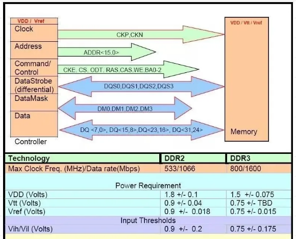
Above Table shows the common technical requirements and proprietary technical requirements of DDR2 memory PCB board and DDR3 memory electronic PCB board which should be notified in the process of PCB reverse engineering.

