

Copy Circuit Board Layer-Up Design
For many consumer products, many companies only give the PCB board thickness, the number of layers and the control impedance value. The Circuit Board Layer-Up Design is carried out by the electronic printed circuit board factory. As the speed of products increases, Copy Circuit Board Layer-Up Design is no longer exclusive to PCB manufacturers, and has become the daily operation of SI signal integrity engineers in many companies. Just like system updates, keeping up with the times is an eternal theme.
In general, three factors are considered in copying Circuit Board Layer-Up Design:
Total thickness (reusability of products & requirements for institutional design)
Determination of the number of layers (signal layer, power plane layer & ground plane layer)
Symmetry (easy to control in PCB production)
The figure below shows the Circuit Board Layer-Up design recommendations for a certain type of Electronic PCB board given by Intel. Whether it is 8 layers or 10 layers, generally only the power plane layer or PP is fine-tuned.

From a electronic pcb card cloning signal integrity perspective, the stack-up design typically chosen is as follows:
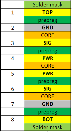
Each trace layer has a GND reference plane layer to ensure the integrity of the signal return path, thereby ensuring the integrity of the signal.
There are various products. In the face of various products, the difference in the number of layers of the wiring layers is the biggest variable in the stacking of the same thickness and total number of layers.
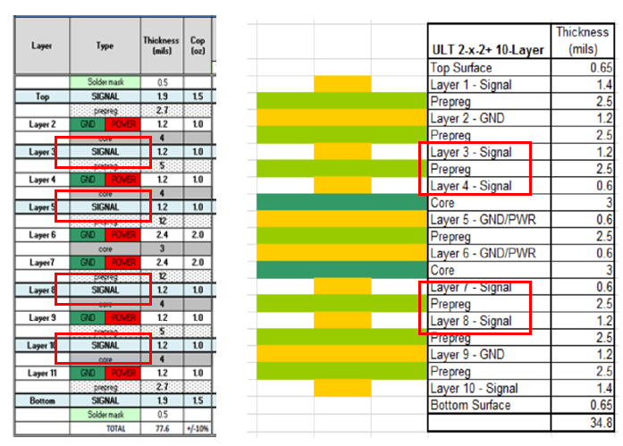
The above picture shows the different stack designs generated by Intel for different products, giving the same 4 layers pcb board.