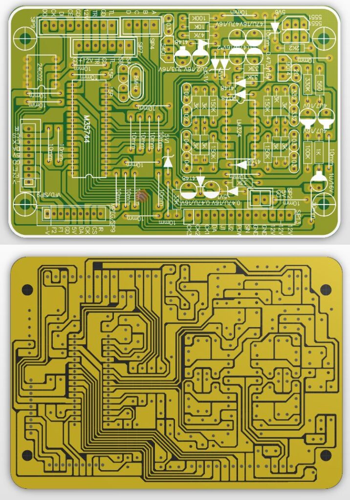
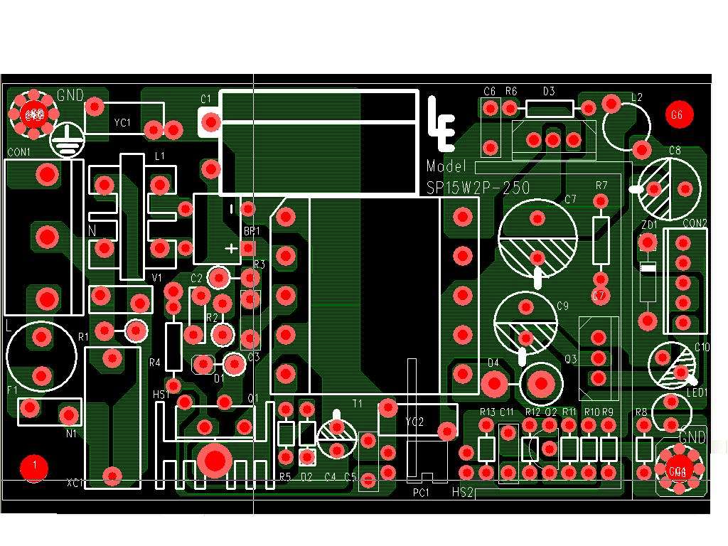
Cloning PCB Board Process
During Cloning PCB Board process, after the printed circuit board schematic drawing recreation is completed, the PCB diagram should be reviewed to see whether the electronic PCB card relayout is reasonable and whether the optimal effect can be achieved. It can usually be investigated from the following aspects:
1. Does Cloning PCB Board Process ensure that the wiring is reasonable or optimal, whether it can ensure the reliable operation of the wiring, and whether the reliability of the circuit board electricity operation can be guaranteed. In the PCB layout reverse engineering, it is necessary to have an overall understanding and planning of the direction of the signal, as well as the power supply and ground wire network.

2. Whether the size of the printed circuit board is consistent with the size of the processing drawing, whether it can meet the requirements of the PCB manufacturing process, and whether there is a behavior mark.
This point requires special attention. The circuit diagram layout and wiring of many PCB boards are cloned very beautifully and reasonably, but the precise positioning of the positioning connector is neglected, resulting in the design of the circuit board cannot be docked with other circuits.

3. Whether the components conflict in two-dimensional and three-dimensional space. Pay attention to the actual size of the device, especially the height of the device. When welding components without layout from PCB board cloning, the height should generally not exceed 3mm.

