Circuit Board Reverse Engineering Process
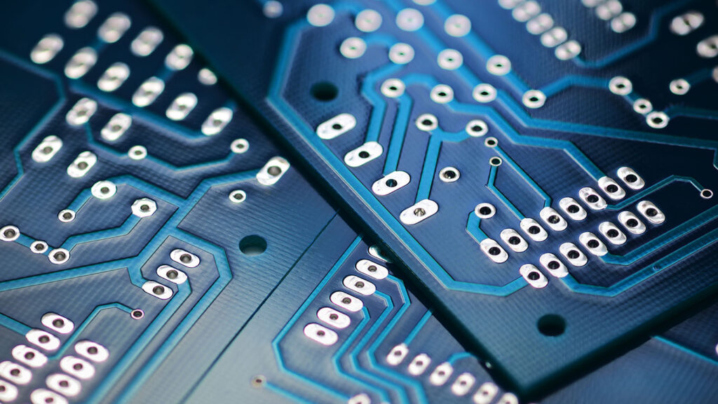
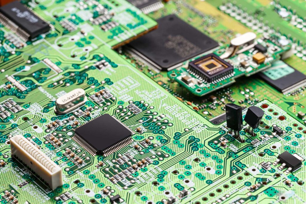
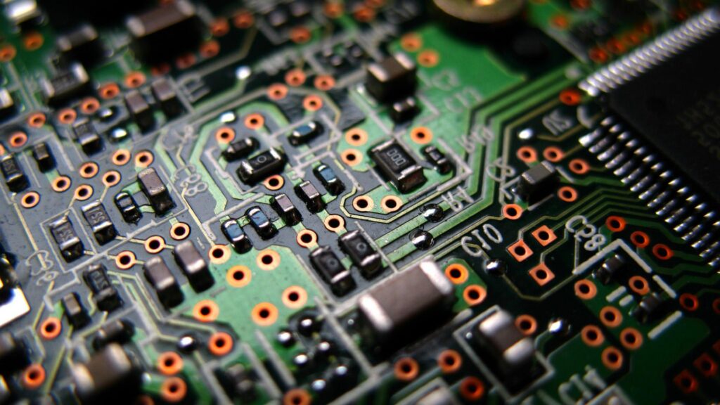
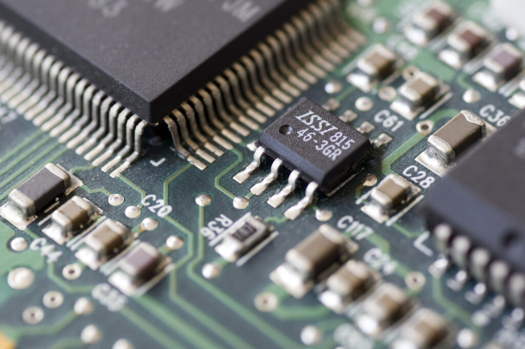
In the process of Circuit Board Reverse Engineering, a physical PCB circuit board is utilized to generate fabrication and design data including schematic diagram, layout drawing, gerber file, netlist file and BOM List,.

Reverse engineering is a process that begins with the operator re-creating the product’s PCB design data from scratch using an existing artefact. It is not essential to collect circuit board design data in a harmful manner in order to steal intellectual property.
The RE process generates data that can be used to troubleshoot, repair, redesign, and remanufacture an electronic PCB card device, as well as to evaluate its security for use in a restricted environment. The data generated by the RE process can be utilised for several purposes.

Because of the importance of keeping spare and replacement parts on hand for systems that have outlived their intended lifespan, the government has established entire departments to regulate and plan for the ultimate obsolescence of these systems and their parts.

Material shortages can lead to DMS/DMSMS when demand for obsolete parts outstrips supply. Among the most prominent areas of obsolescence in technical systems are medical imaging systems and numerous military technology.

Tags: engenharia reversa placa de circuito impresso arquivo cad,engenharia reversa placa de circuito impresso arquivo gerber,engenharia reversa placa de circuito impresso desenho de layout,engenharia reversa placa de circuito impresso diagrama esquemático,engenharia reversa placa de circuito impresso lista de materiais

