Reverse Engineering PCB
-
Projector PCB Board Reverse Engineering
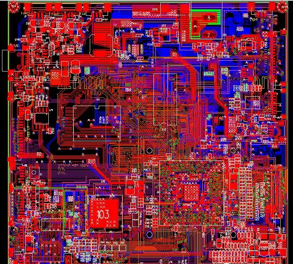
Projector PCB Board Reverse Engineering will be able to extract schematic diagram, netlist from original printed circuit board, through schematic drawing to restore electronic projector circuit board layout diagram, gerber file, and de-solder the co...
-
Electronic PCB Board Gerber File Cloning
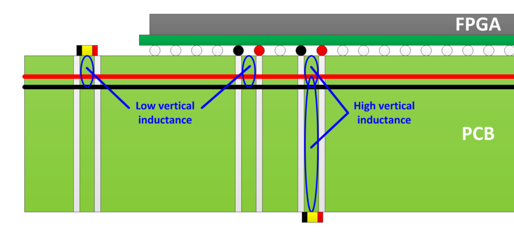
In high-speed Electronic PCB Board Gerber File Cloning, there will inevitably be parasitic inductance, parasitic resistance and parasitic capacitance, so the high-frequency noise will eventually be coupled to other circuits, and the presence of para...
-
Reverse Engineering PCB Board Layout Drawing Common Mistakes
There are some common mistakes in the process of Reverse Engineering PCB Board Layout Drawing, (1) There is no signal connected to the ERC report pin: I/O attributes are defined for the pins when the package is created, Inconsistent grid attr...
-
HDI Circuit Board Layout Cloning
Digital circuits often require discontinuous currents, so inrush currents are generated for some HDI Circuit Board Layout cloning. If the power trace is very long, the presence of inrush current will cause high-frequency noise which can be effective...
-
PCB Board Gerber File Cloning to connect signal wire to ground wire
There are various ways to connect signals to ground and PCB Board Gerber File Cloning is one of them, through Circuit board redesigns where components are randomly connected to the ground point will generate high ground inductance and cause unavoida...
-
PCB Board Low Inductance Grounding System Application
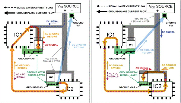
PCB Board Low-inductance grounding systems are the most important factor in minimizing EMC problems through PC Board reverse engineering. Maximizing the grounding area on the PCB circuit board can reduce the system grounding inductance, thereby redu...
-
PCB Board Reverse Engineering Service Cost Estimation
PCB Board Reverse Engineering Service Cost Estimation should be based on the complexity of the cloned PC board and the number of piece-parts/components involved. The total effort involved is dependent upon the technical data available versus the amo...
-
How to Test Cloned PCB Board Functionality
The final purpose of PCB board reverse engineering is to re-manufacture the physical printed circuit board according to the gerber file, layout diagram and BOM List, schematic diagram extracted. and test cloned PCB board according to below steps: ...
-
Electronic PCB Board Gerber File Relayout
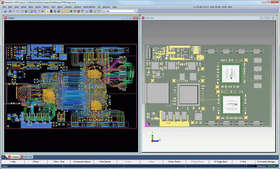
The optimization of Electronic PCB Board Gerber File Relayout in terms of grounding, decoupling, and signal routing and can be used as a model when laying out the ADC section of the PC board in a system. The actual evaluation over circuit board layo...
-
Electronic PCB Board Layout Diagram Design
Electronic PCB Board Layout Diagram Design are by far the most common method of assembling modern electronic circuits. Comprised of a sandwich of one or more insulating layers and one or more copper layers which contain the signal traces and the pow...


