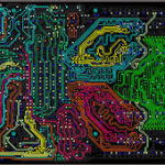
Reverse Engineering PCB
-
PCB Board Reverse Engineering Tools
In recent days, pcb board reverse engineering tools have made some new breakthrough, some of the analysis tools have been developped regarding to the high speed design issue and pcb board reverse engineering. Take the software from INNOVEDA as the si...
-
ESD effect when Clone PWB Board
Clone PWB Board need to prevent the negative effect of ESD on them, in order to minimize the negative effect and have a better PWB Board clone outcome, below measures must be made to ensure the goal being achieved: 1. cabinet grounding track on the t...
-
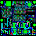
Reverse Engineering SMT PCB Pads Layout
Reverse Engineering SMT PCB Pads Layout must take below consideration into account: engenharia reversa SMT PCB Pads Layout deve levar em consideração abaixo 1> SMT components on the wave soldering flow side, the bigger size component pad su...
-
SMT PCB Reverse engineering Principle
1 The electronic components placement of SMT PCB Reverse engineering 1> when SMT PCB being placed on the convey strap of reflow oven, the longer axis of component should be reverse engineeringed to vertical to the orientation of conveying. Whi...
-
Printed Circuit Board Reverse Engineering For Electro-Magnetic Compatibility
Printed Circuit Board Reverse Engineering for electro-magnetic compatibility Reverse Engineering Printed circuit board need to take the electro-magnetic compability issue into consideration. Electro-magnetic compatibility means the system or device l...
-
Bayer expands production for coating raw materials in China
Bayer MaterialScience is increasing its production capacities in the Asia/Pacific region to meet the continued growth in demand there for raw materials for coatings and adhesives. Ground has been broken at the site in Shanghai, China, for a new plant...
-
PCB Board Reverse Engineering Inspection
PCB Board Reverse Engineering Inspection includes the inspection against track on top and bottom layer and tracks on the power supply and signal transmission, as well as the soldering pad and socket/terminals/marks: A inspeção de engenharia rever...
-
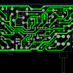
Cloning PCB Card
Most of the engineers will consider the layout of each layer when Cloning PCB card, and often be confused by whether the signal layer or groundling layer should be Cloning and if the signal layer and groundling layer should placed in turns or in a c...
-
NCAB Group Germany appoints new Managing Director
PCB supplier, NCAB Group Germany, with headquarters in Sweden, has appointed Heinie von Michaelis as their new Managing Director. “We are very pleased that Heinie von Michaelis has joined us”, says Hans Ståhl, CEO NCAB Group. “With ...