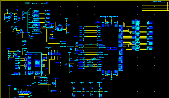
Reverse Engineering PCB
-
Printed Circuit Board Duplication
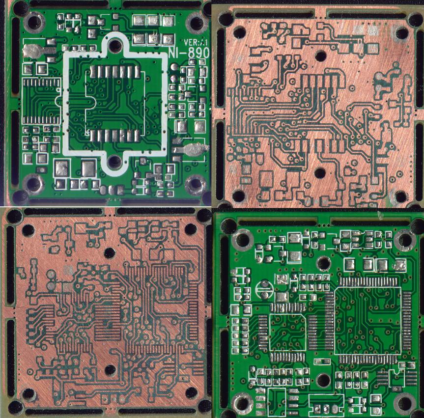
Printed Circuit Board Duplication are other terms for cloning PCB board layout diagram and gerber file, such as “PCB copy” and “PCB duplicate.” Reverse engineering is the technique of taking an existing printed circuit board ...
-
Circuit Board Reverse Engineering Process
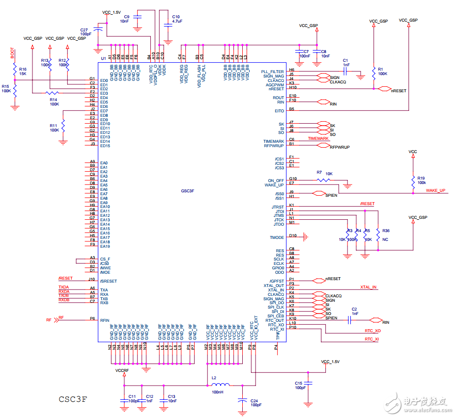
In the process of Circuit Board Reverse Engineering, a physical PCB circuit board is utilized to generate fabrication and design data including schematic diagram, layout drawing, gerber file, netlist file and BOM List,. In the process of Circuit...
-
Cloning Circuit Board Introduction
Cloning Circuit Board has no software; therefore, it can only be measured and drawn using calliper edge, which it’s quite sluggish, and its precision is also bad. However, it is extremely easy to replicate the PCB board with the program. Gener...
-
Electronic PCB Reverse Engineering Services
We are a leading provider of electronic PCB reverse engineering services. Our team has more than ten years of combined experience in reverse engineering electronic equipment, so we are well-equipped to face any problem that comes our way. We are...
-
PCB Reverse Engineering and how to Reverse Engineer a PCB
Reverse engineering plays an important role in industries in different sectors, mainly in the printed circuit boards. PCB Reverse Engineering is the multilayered process where there is inclusion of PCB research, reverse analysis and PCB design for r...
-
Clone PCB Board Component Layout Drawing
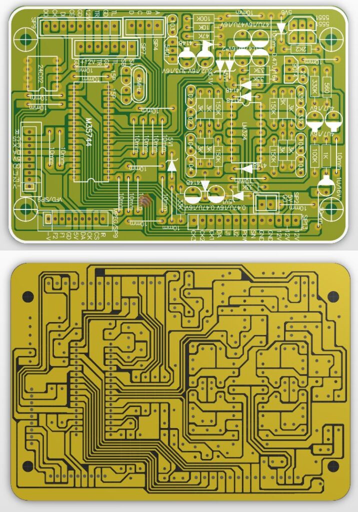
Clone PCB Board Component Layout Drawing is another very important step for PCB Clone service, below there are several points need to be clarified in the process: 1. Whether the layout of the components is dense and orderly, neatly arranged, and ...
-
Cloning PCB Board Process
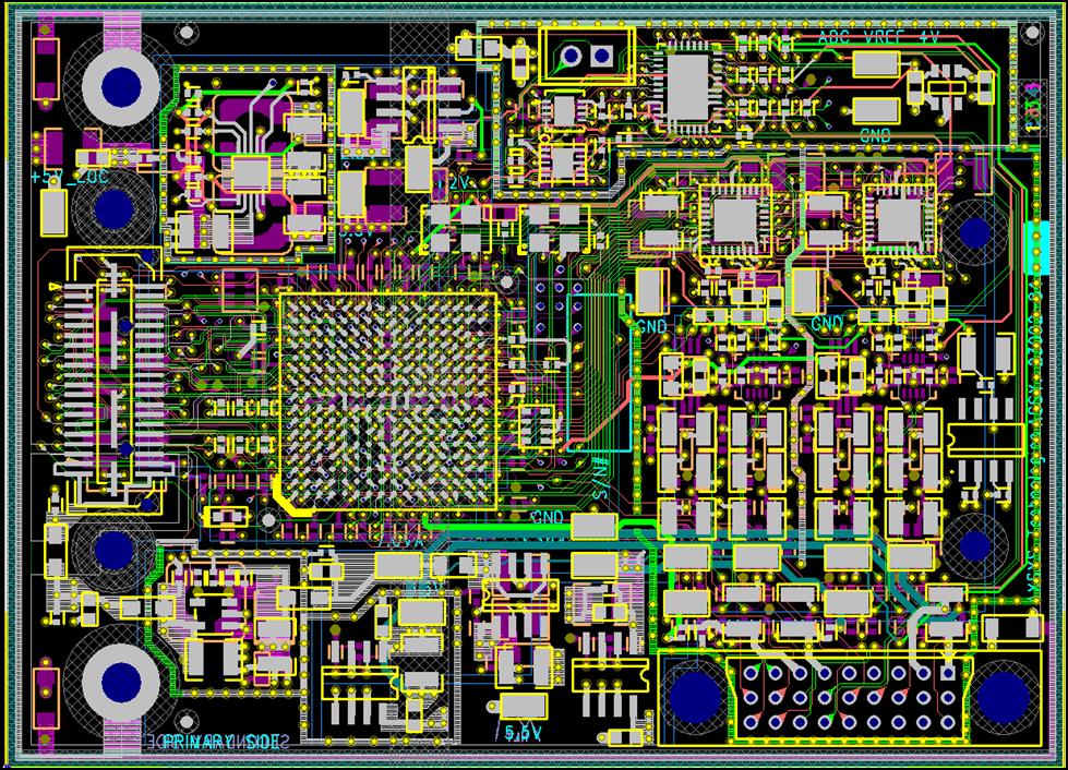
During Cloning PCB Board process, after the printed circuit board schematic drawing recreation is completed, the PCB diagram should be reviewed to see whether the electronic PCB card relayout is reasonable and whether the optimal effect can be achie...
-
Clone Digital Circuit PCB Board Schematic
When we clone Digital Circuit PCB Board Schematic, the propagation of a digital signal is from one logic gate to another logic gate. The signal is sent from the output end to the receiving end through a wire. When we clone Digital Circuit PCB Bo...
-
GPS Module Circuit Board Reverse Engineering
GPS Module Circuit Board Reverse Engineering can extract embedded schematic diagram out from it and then recreate layout drawing, netlist, Gerber file, list of components can be built according to the parts applied on it; GPS Module Circuit Board...
-
Projector Circuit Board Cloning
Projector Circuit Board Cloning is to help client re-manufacture the electronic PCB card of projector, hereby mainly refers to mainboard, restore PCB board layout diagram and gerber file in order to re-manufacture it; Projector Circuit Board Clon...


