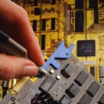
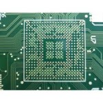
Reverse Engineering PCB
-
PCB Board Reverse Engineering Topology Plan
Engineer needs to use topology plan, through the interaction of components on the already finished layout and semi-finished layout to achieve the best layout and interconnection, as a result of that, to improve the PCB board reverse engineering effic...
-
PCB Reverse Engineering Topology Plan
Engineer can use IP and furthermore, the application of topology plan and layout tools to support the IP, consequently finish the whole PCB reverse engineering process. Engineer’s responsibility is through layout as few necessary components as possib...
-
Grounding Solution for Printed Circuit Board Reverse Engineering
In this section we discuss grounding. This is undoubtedly one of the most difficult subjects in Printed circuit board reverse engineering. While the basic concepts are relatively simple, implementation is very involved. For linear systems the ground ...
-
PCB Reverse Engineering Dimension Analysis
Dimensional analysis of PCB Reverse Engineering: 1 Dimensional analysis of PCB reverse engineering‘s objective is to define the size and shape of the parts and locate all part features, these parts include the electronic and mechanical. Toler...
-
Transmission Line Technique by PCB Reverse Engineering
Transmission Line Technique by PCB Reverse Engineering The only way to preserve 1 ns or less rise/fall times over distances greater than about 2 inches without ringing is to use transmission line techniques by by PCB Reverse Engineering. below Figure...
-
Analog Circuit Protection From Printed Circuit Board Reverse Engineering Technique
Analog Circuit Protection From Printed Circuit Board Reverse Engineering Technique The best ways to keep sensitive analog circuits from being affected by fast logic through Printed Circuit Board Reverse Engineering technique are to physically separat...
-
High Speed Logic in PCB Board Reverse Engineering
High Speed Logic in PCB Board Reverse Engineering Much has been written about terminating PCB traces in their characteristic impedance, to avoid signal reflections after PCB Board Reverse Engineering. A good guideline to determine when this is necess...
-
Embedded Traces on PCB Reverse Engineering
As we all know that allow the PCB traces of defined impedance has been allowed in PCB Reverse Engineering , either on a surface layer or embedded between layers. There of course are many other considerations beyond these impedance issues. Embedded si...
-
PCB Reverse Engineering Hardware Analysis
PCB Reverse Engineering Hardware Analysis is one of the most important steps for completion of this work. PCB Reverse Engineering Hardware Analysis can made things better clear. A hardware analysis should be performed during the stage of PCB reverse...
-
Route Layout Drawing of PCB Reverse Engineering
There are a lot of routing tools, such as Autoroute, that are very tempting to use when routing the board. It is very important however that at least the important nets are routed by hand, and after autorouting, you must change some nets around and m...