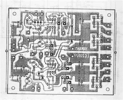
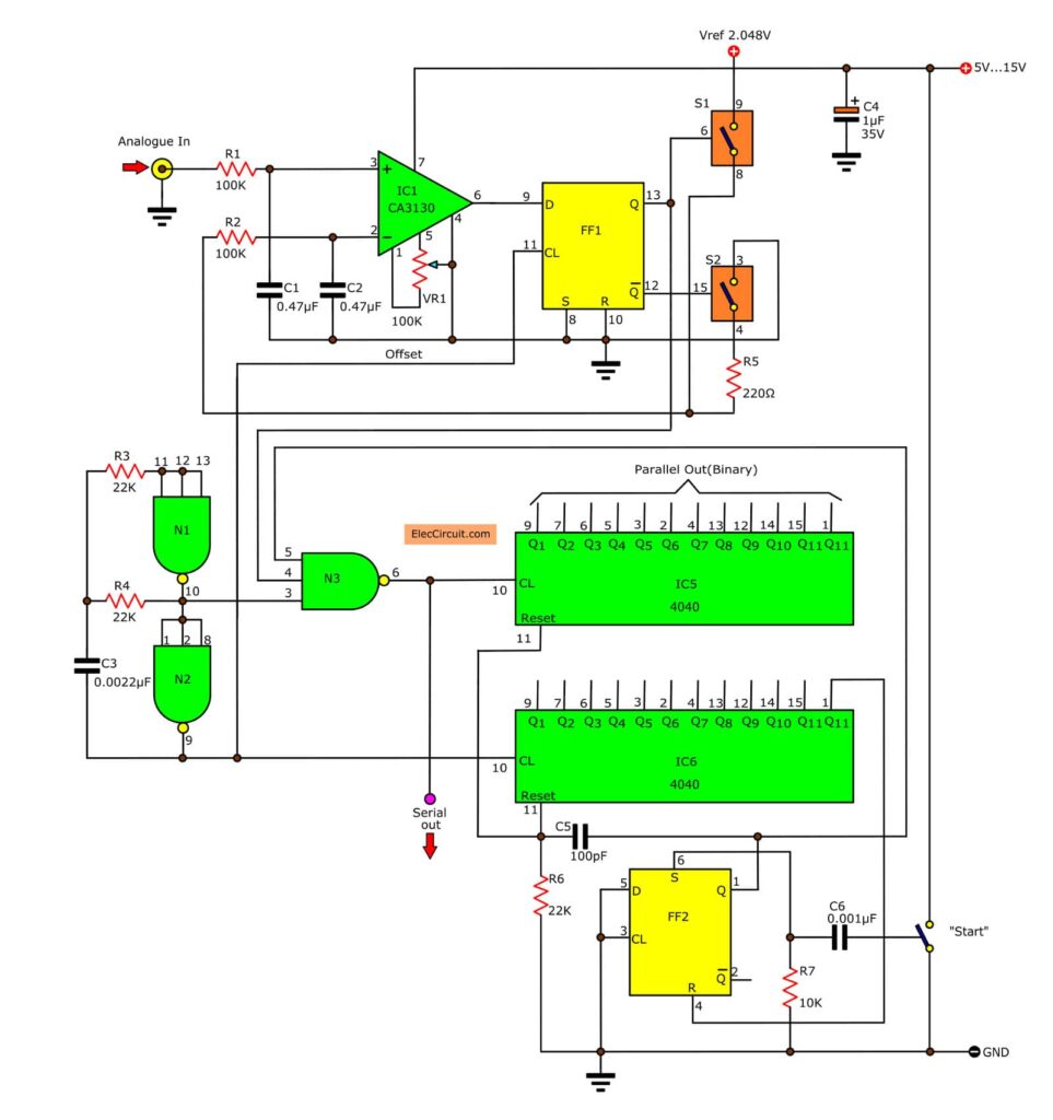
Reverse Engineering PCB
-
Redesign PCB Board Layout Diagram Procedures
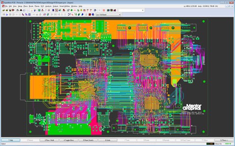
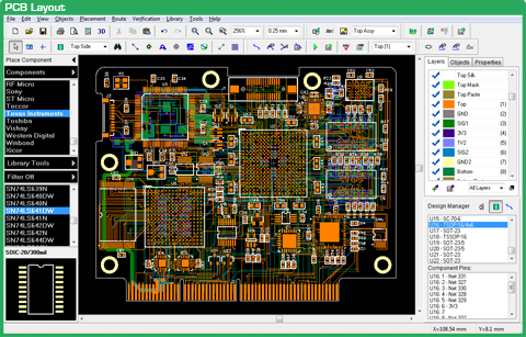
Redesign PCB Board Layout Diagram is a reverse engineering process which will start from desolder electronic/mechanical components off the PC board, and then we are going to require design components on the newly cloned PCB layout drawing, 1, U...
-
Reverse Engineering PCB Board Layout Diagram Guidelines
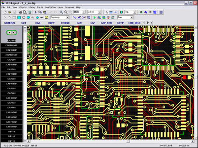
Reverse Engineering PCB Board Layout Diagram Guidelines is critical for printed circuit board cloning since it will ensure the correctiveness of the Gerber file; Reverse Engineering PCB Board Layout Diagram Guidelines is critical for printed circ...
-
Bypass Capacitor Used in PCB Circuit Board Gerber File Rerouting
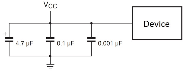
Bypass capacitor is playing an important role in the PCB circuit board gerber file rerouting, the bypass capacitors can be placed in the following two positions on the pcb circuit board gerber file: one capacitor (10µF to 100µF) is placed on the pow...
-
Circuit Board Wiring Schematic Reverse Engineering
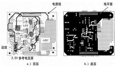
Circuit Board Wiring Schematic Reverse Engineering can improve the conversion result after adding a fourth-order anti-aliasing filter to the circuit. In addition, a ground plane has been added to the circuit board wiring schematic. The wiring shown ...
-
Reverse Engineering Circuit Board Wiring Design Ground & Power Strategy
Reverse Engineering Circuit Board Wiring Design Ground & Power Strategy can determine the general location of the electronic components, the ground plane and power plane can be defined. Realizing these planes requires some strategic skills. R...
-
12 Bit Sensing System PCB Board Wiring Diagram Cloning
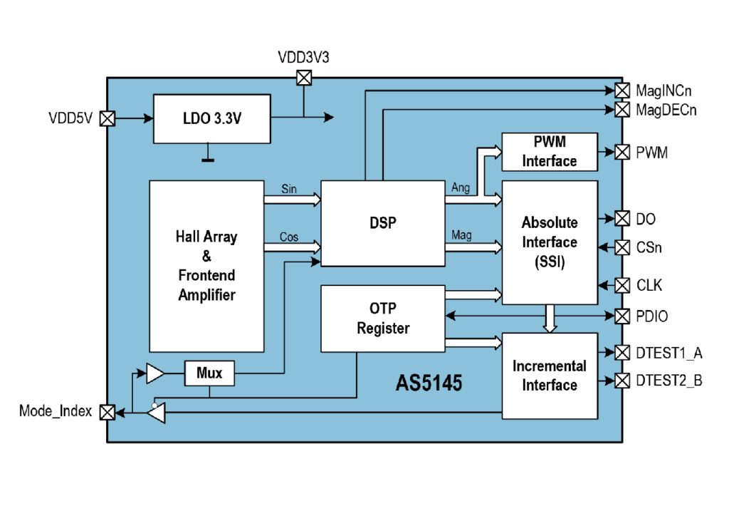
For 12 Bit Sensing System PCB Board Wiring Diagram Cloning, the applied circuit is a load cell circuit that can accurately measure the weight applied to the sensor, and then display the result on the LCD display. 12 Bit Sensing System PCB Board W...
-
Reverse Engineering PCB Board Schematic to avoid Power Supply Noise
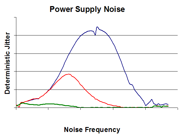
Reverse Engineering PCB Board Schematic to decrease Power Supply Noise, extract printed circuit board wiring diagram from physical PCB board sample for a better performance; Reverse Engineering PCB Board Schematic to decrease Power Supply Noise, ...
-
Inverter PCB Board Gerber File Reverse Engineering
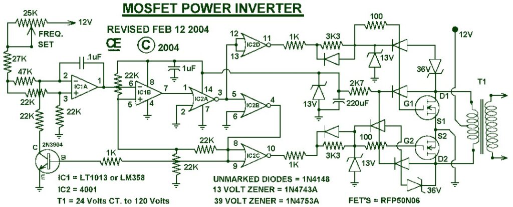
For all these Inverter PCB Board Gerber File Reverse Engineering, the power strategy should be to connect all ground, positive and negative power pins to the analog plane when design analog and digital circuitry. Inverter PCB Board Gerber File Re...
-
Power Supply PCB Board Layout Reverse Engineering
For Power Supply PCB Board Layout Reverse Engineering, two ground pins are usually derived from the chip: AGND and DGND. The power supply has a lead-out pin. For Power Supply PCB Board Layout Reverse Engineering, two ground pins are usually deriv...
-
Converter Circuit Board Gerber File Reverse Design
Converter Circuit Board Gerber File Reverse Design can help engineer to reverse engineering PCB gerber file to figure out the electrical connection relationship among components, uses the charge distribution formed by the capacitor array. Convert...


