Articles
-
Printed Circuit Board Cloning Tools
Printed Circuit Board Cloning Tools including a combination of hardware and software. Here’s a detailed list of the essential tools you’ll need: Printed Circuit Board Cloning Tools including a combination of hardware and software Hardware Tool...
-
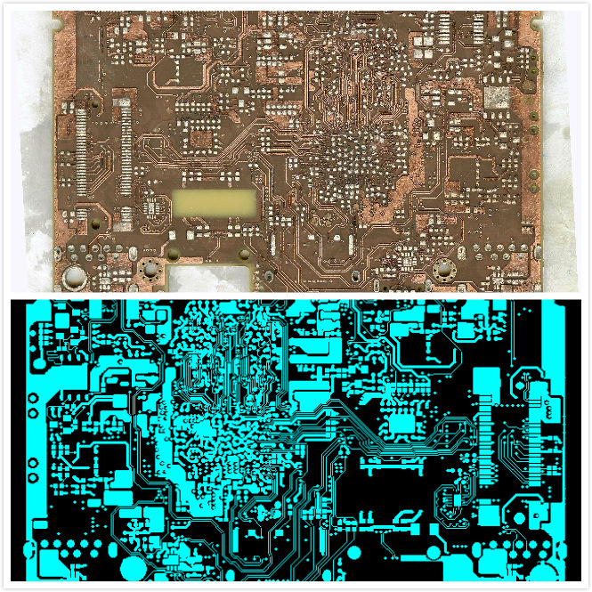
Printed Circuit Board Layout Cloning
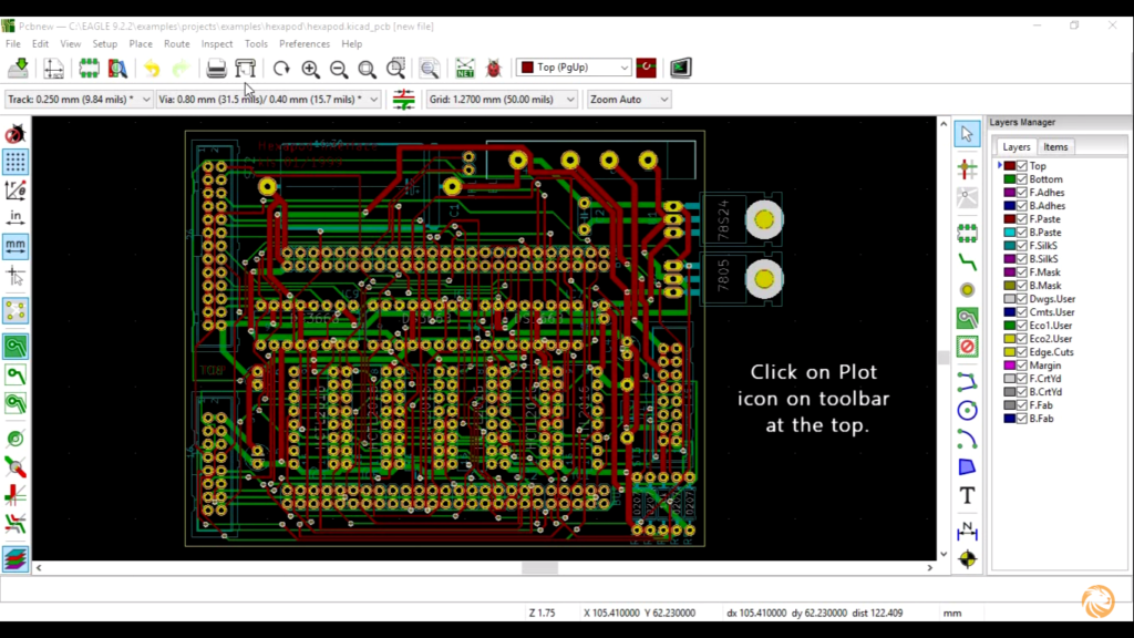
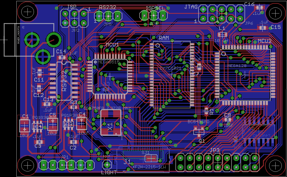
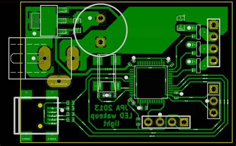
Printed Circuit Board Layout Cloning is a process to place electronic components on the PCB board design drawing which has been created through schematic diagram, the re-layout is to put electronic components on the circuit board. At this time, if a...
-
Check PCB Board Quality Methods
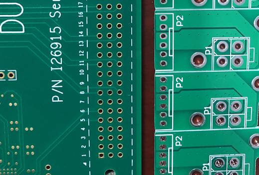
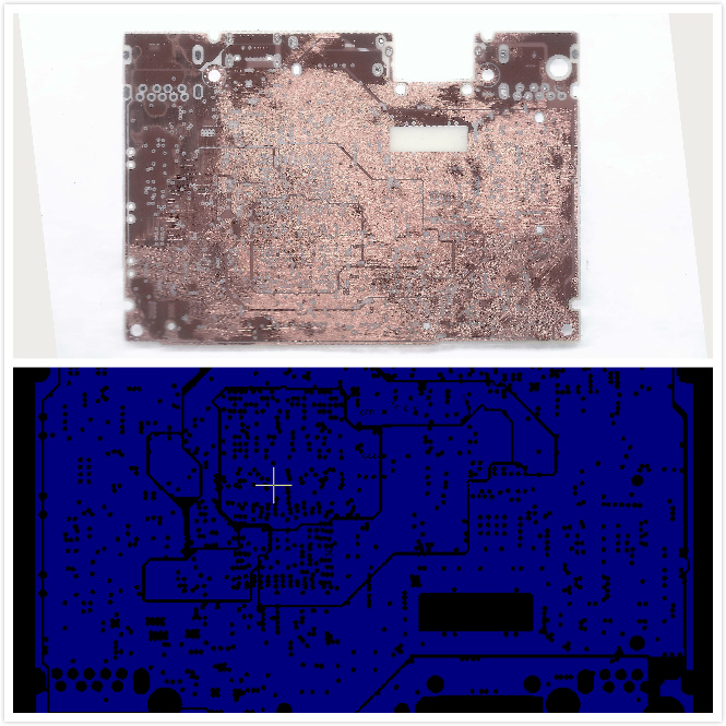
There are several simple ways through checking the appearance of electronic PCB boards can determine the quality of it, since cloning PCB board needs to strip off the solder resist mask and fully expose the copper circuitry pattern under it, then dr...
-
PCB Board Development History
The PCB Board has been the basic building block of electronic devices since the beginning of the modern electronic age, just after the Second World War. Because of the circuit board’s unique ability to create large numbers of connections at a single...
-
Multilayer PCB Board Characteristic
Among them, the Multilayer PCB Board refers to a printed board with more than two layers. It is composed of connecting wires on several layers of insulated substrates and pads for assembling and soldering electronic components. Multilayer PCB Bo...
-
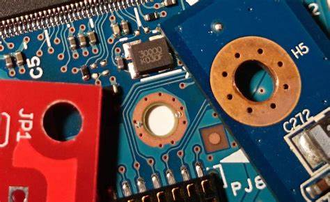
PCB Mounting Holes Design
PCB mounting holes help to fix the PCB to the housing. But this is its physical and mechanical purpose. In addition, in terms of electromagnetic functions, PCB mounting holes can also be used to reduce electromagnetic interference (EMI), as a result...
-
Reverse Engineering Electronic Circuit Board Layout Drawing for Signal Integrity
Reverse Engineering Electronic Circuit Board Layout Drawing for Signal Integrity, and the most frequent signal integrity problems includes mainly include signal reflection, crosstalk, signal delay, and timing errors. Reverse Engineering Electron...
-
Redrawing PCB Board Layout Diagram to reduce Electronic Magnetic Interference
The three major elements of EMC, interference sources, transmission channels and sensitive devices. Therefore, Redrawing PCB Board Layout Diagram to reduce Electronic Magnetic Interference starts with eliminating interference sources, cutting off th...
-
Noise interference from power supply
Copy original PCB Board scheme drawing and modify it to reduce noise interference from power supply, this is a reverse engineering process through which the original printed circuit card schematic diagram and layout file/gerber file will be restore...
-
Reverse Engineer Circuit Board Power/Ground/Signal Layout Pattern
After placing the components, the job will enter the process of Reverse Engineer Circuit Board Power/Ground/Signal Layout Pattern, you can place power, ground, and signal traces to ensure that your signal has a clean and trouble-free path. Rever...


