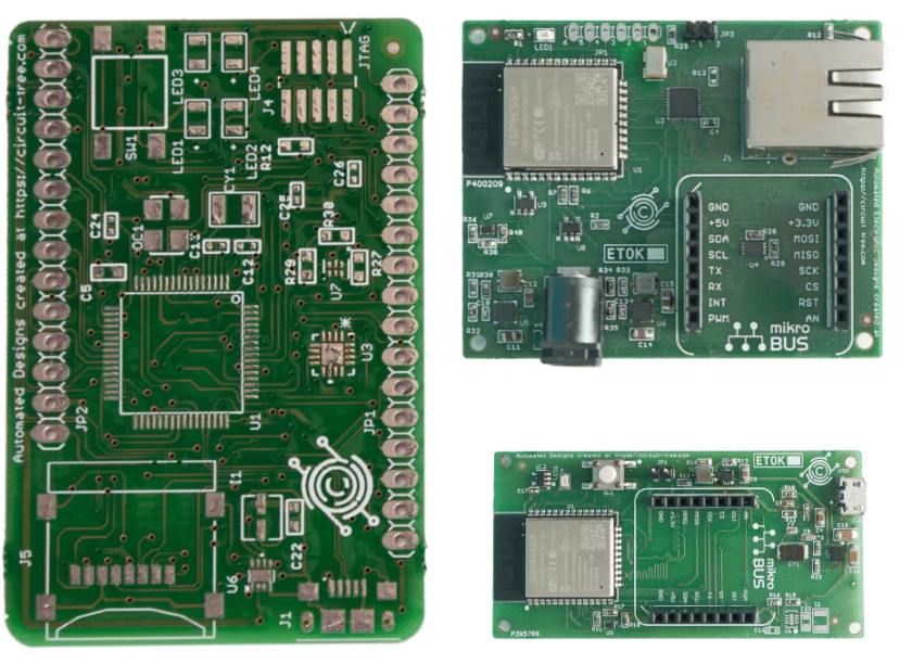
Automation Control Mainboard Reverse Engineering Service
For a Automation Control Mainboard which has been constrained by the number of PCB layers (such as a 4-layer board), all of its signal lines can only go on the TOP and BOTTOM layers. The middle two layers, one of which is the GND plane layer, and the other layer is VDD plane layer, Vtt and Vref are routed on the VDD plane layer.

When we carry on automation control mainboard reverse engineering service, 6 layers might be considered for printed circuit board scheme rewiring, it becomes easier to design a dedicated pcb board topology. At the same time, the distance between the Power layer and the GND layer is reduced, thereby improving power integrity.
The impedance of another parameter of the interconnection channel must be constant and continuous during the design of DDR2. The impedance matching resistance of single-ended traces of 50 Ohms must be used for all single-ended signals, and impedance matching must be achieved. For differential signals, 100 Ohms terminal impedance matching resistance must be used for all differential signal terminals, such as CLOCK and DQS signals.
In addition, all matching resistors must be pulled up to VTT and maintained at 50 Ohms, and the ODT setting must also be maintained at 50 Ohms. In the design of DDR3, the terminal matching resistance of single-ended signals between 40 and 60 Ohms can be selectively designed to the ADDR/CMD/CNTRL signal line, which has proven to have many advantages.
Moreover, the terminal matching resistance pulled up to VTT may need to be selected differently according to the trace impedance of the SI simulation result, and the resistance value is usually between 30-70 Ohms. The impedance matching resistance of the differential signal is always 100 Ohms.

