Reverse Engineering a PCB using KiCad Software
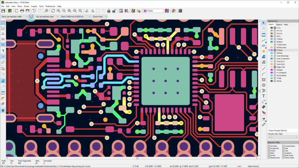
Open-source PCB design software KiCad that can be used for Reverse Engineering a PCB by recreating layout drawing, gerber file and schematic diagram.

Reverse engineering a PCB using KiCad involves several steps, from documenting the existing PCB to recreating the schematic and layout in the software. Here’s a detailed guide to help you through the process:
Step 1: Preparation
- Disassemble the PCB: Carefully remove any components from the PCB using a desoldering station. Note down the placement and orientation of each component.
- Document the PCB: Take high-resolution photos of both sides of the PCB. Ensure all traces and component labels are visible.
Step 2: Install and Set Up KiCad
- Download and Install KiCad: If you don’t have KiCad installed, download and install it from the official website.
- Create a New Project: Open KiCad and create a new project. Name it appropriately.
Step 3: Reconstruct the Schematic
- Open Eeschema: This is the schematic capture tool in KiCad. You can access it from the main project window.
- Add Components: Use the Add Symbol tool to place components on your schematic. Refer to your photos and notes to place the components accurately.
- Connect Components: Use the Wire tool to draw connections between components based on the PCB traces you documented. This will create the schematic diagram.
- Annotate Schematic: Use the Annotate Schematic tool to assign unique identifiers to each component.
- Perform Electrical Rules Check (ERC): This helps to identify any errors in the schematic.
Step 4: Printed circuit board Layout Design cloning
- Generate Netlist: From the schematic editor, generate a netlist by clicking on the Generate Netlist button.
- Open PCBNew: This is the PCB layout tool in KiCad. You can access it from the main project window.
- Import Netlist: In PCBNew, import the netlist you generated. This will place all the components on the board layout area.
- Arrange Components: Place the components on the board layout according to their positions on the original PCB.
- Route Traces: Use the Route Tracks tool to draw the PCB traces, replicating the paths from the original PCB. Pay attention to the layer assignments (top, bottom, etc.) if it’s a multi-layer PCB.
- Add Edge Cuts: Define the board outline using the Edge.Cuts layer.
Step 5: Verify and Test
- Design Rule Check (DRC): Run the DRC tool in PCBNew to ensure there are no layout errors.
- Generate Gerber Files: If everything is correct, generate the Gerber files for manufacturing. Go to File > Plot and select the necessary layers to generate the Gerber files.
Step 6: Manufacture and Assemble
- Send Gerber Files to Manufacturer: Send the Gerber files to a PCB manufacturer to have the boards produced.
- Assemble the PCB: Once the PCBs are produced, assemble the components and test the board to ensure it functions correctly.
Additional Tips:
- Use Layers: Pay attention to different layers (e.g., top, bottom, inner layers for multi-layer PCBs) when routing traces in PCBNew.
- Component Libraries: Make use of component libraries in KiCad for accurate component placement.
- Keep Detailed Notes: Document each step thoroughly, especially if you plan to make modifications or troubleshoot issues later.
- Utilize KiCad’s Footprint Libraries: For accurate component placement, use KiCad’s extensive footprint libraries or create custom footprints if needed.
By following these steps, you can effectively reverse engineer a PCB using KiCad. This open-source tool provides all the necessary features to accurately recreate both the schematic and layout of the original board.

