Pulse Generator PCB Board Cloning
After we do the principle Pulse Generator PCB Board Cloning and simulation, one thing worth noting in printed circuit board Layout redesign is impedance control.
As we all know, we should try our best to ensure that the characteristic of the trace is 50 ohms, which is mainly related to the line width. In this example, it is two and a half layers. The Surface Coplanar Line model is used in Polar to calculate the impedance, and we can get a set of ideal values: Height(H)=39.6mil,
Track(W)=30mil,
Track(W1)=30mil,
Thickness=1OZ=1.4mil,
Separation(S)=7mil,
Dielectric(Er)=4.2,
The corresponding characteristic impedance is 52.14 ohms, which meets the requirements.
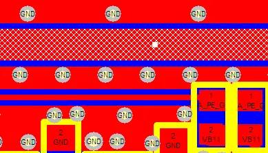
The highlighted line in the figure below is such an RF trace.

Placement of RF components
I believe that anyone who has done Radio frequency pcb card design cloning should know that we should make the length of the traces as short as possible, and the more compact the components are placed, the better (except for special requirements);

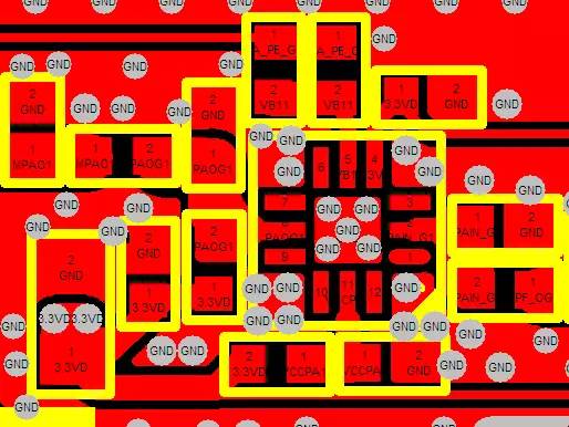
At the same time, we will try our best to ensure that the placement of components is beneficial to the wiring (do not make the wiring go around). As shown in the figure below, it is the placement of the surrounding components of the RF power amplifier (PA, Power Amplifier). We can see that the distance between the components is very small;

Problems that should be paid attention to in RF wiring
As mentioned above, the length of the RF trace should be as short as possible, and the line width should be set strictly according to the calculated value. It is especially important to pay attention to the fact that there should be no sharp points in the RF trace. At the turning point of the trace, it is best to use an arc, as shown in the figure below.
Secondly, in the cloning of multi-layer circuit boards, it is possible that important RF lines will inevitably cross, and then we will use the last thing we want: vias. In this way, some Radio frequency signal lines will go to the bottom layer or even the middle layer, but no matter which layer it is, the RF traces must have a reference plane. At this time, a noteworthy problem is not to cross layers, or not to make the ground plane different. continuous.

