Reverse Engineering Circuit Board Layout to Improve Heat Dissipation
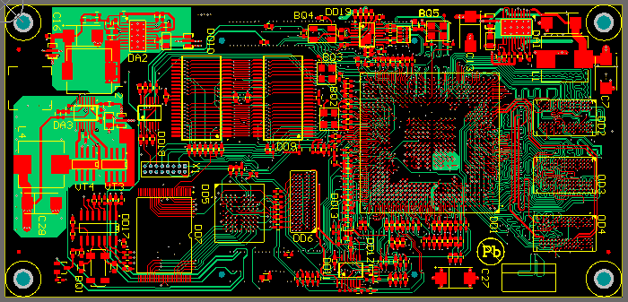
Reverse Engineering Circuit Board Layout to Improve Heat Dissipation. Because the resin in the plate has poor thermal conductivity, and the copper foil lines and holes are good heat conductors, increasing the remaining rate of copper foil and increasing the quantity of heat conduction holes are the main means of heat dissipation, above methods need to reverse engineering original printed circuit board and redesign its layout drawing;
To evaluate the heat dissipation capacity of the PCB, it is necessary to calculate the equivalent thermal conductivity (nine eq) of the composite material composed of various materials with different thermal conductivity-the insulating substrate for the PCB.

The components on the same printed circuit board should be arranged as far as possible according to their calorific value and degree of heat dissipation. Electronic component with low calorific value or poor heat resistance (such as small signal transistors, small-scale integrated circuits, electrolytic capacitors, etc.) should be placed in the cooling airflow.
The uppermost flow (at the entrance), the devices with large heat or heat resistance (such as power transistors, large-scale integrated circuits, etc.) are placed at the most downstream of the cooling airflow. In the horizontal direction: high-power devices are arranged as close to the edge of the printed circuit board as possible to shorten the heat transfer path.

In the vertical direction: high-power devices are arranged as close to the top of the printed board as possible to reduce the impact of these electronic components on the temperature of other devices when they work.

