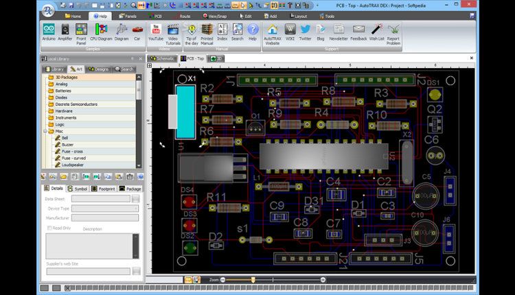
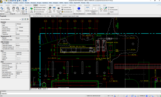
PC Board Schematic Diagram Reverse Engineering Category
In general, PC Board Schematic Diagram Reverse Engineering can be divided into two broad categories—those that most noticeably affect the static or dc operation of the circuit, and those that most noticeably affect dynamic or ac circuit operation, especially at high frequencies.

Another very broad area of PCB Board Schematic Diagram Reverse Engineering is the topic of grounding. Grounding is a problem area in itself for all analog and mixed signal pcb board designs, and it can be said that simply implementing a PCB based circuit doesn’t change the fact that proper techniques are required.
Fortunately, certain principles of quality grounding, namely the use of ground planes, are intrinsic to the PCB board design environment. This factor is one of the more significant advantages to reverse engineering printed circuit board based analog designs, and appreciable discussion of this section is focused on this issue.

Some other aspects of grounding that must be managed include the control of spurious ground and signal return voltages that can degrade performance. These voltages can be due to external signal coupling, common currents, or simply excessive IR drops in ground conductors. Proper conductor routing and sizing, as well as differential signal handling and ground isolation techniques enables control of such parasitic voltages.

