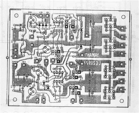
Power Supply PCB Board Layout Reverse Engineering
For Power Supply PCB Board Layout Reverse Engineering, two ground pins are usually derived from the chip: AGND and DGND. The power supply has a lead-out pin.

When using these chips to implement printed circuit board layout redesign, AGND and DGND should be connected to the analog ground plane. The analog and digital power pins should also be connected to the analog power plane or at least to the analog power rail, and appropriate bypass capacitors should be connected as close as possible to each power pin.
For devices like MCP3201, there is only one ground pin and one positive power supply pin. The only reason is due to the limitation of the package pin count.
However, isolating the ground can increase the probability that the converter has good and repeatable accuracy

