eGaN FET Effect in PCB Reverse Engineering
eGaN FET Effect in PCB Reverse Engineering
With the significant reduction in package parasitics provided by the eGaN FET Effect in PCB Reverse Engineering, the common source inductance is minimized and is no longer the major parasitic loss contributor. The high frequency loop inductance, controlled by PCB layout becomes the major contributor to loss, making layout of the eGaN FETs critical to high frequency performance.

eGaN FET Effect in PCB Reverse Engineering
To verify this, different layouts with similar common source inductance and different high frequency loop inductances are compared and methods to reduce loop inductance by PCB layout are proposed.
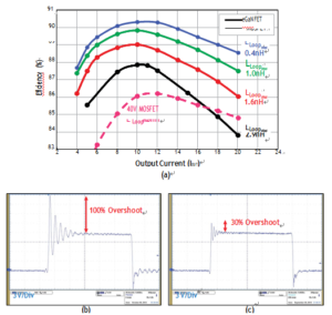
From the efficiency curves obtained from experimental prototypes, shown in figure 3a, the impact of layout on efficiency can be seen for the eGaN FET at 1 MHz. An increase in the high frequency loop inductance from around 0.4 nH to 2.9 nH results in additional loss, decreasing efficiency by over 4%.
Another disadvantage of high frequency loop inductance is that voltage overshoot increases with loop inductance. Decreasing the high frequency loop inductance results in lower voltage overshoot, increased input voltage capability, and reduced EMI.
Below Figures show the switching node waveforms for designs with a high frequency loop inductance of 1.6 nH and 0.4 nH; the voltage over-shoot is reduced from 100% of the input voltage to 30%, respectively.


