Impact of Stray Inductance on PCB Reverse Engineering
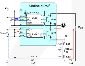
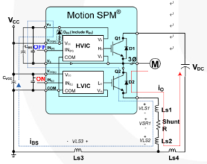
High switching noise may cause a failure in an inverter system. Whenever the IGBT turns on and off, surge voltage is induced due to Stray Inductance on PCB Reverse Engineering of main current paths on the board. below Figures include Ls1 and Ls2, which is stray inductance in PCB layout. High di /dt occurs at
below Figure shows low-side gate current (iGL) path through the gate to the emitter of IGBT Q2 and LVIC and VCC to LO when the low-side input signal is on. The low-side IGBT gate charging path includes parasitic inductances and a shunt resistor because LVIC VSL is not connected to the emitter of Q2.
and it is regarding bootstrap current path (iBS) through the collector to the emitter of IGBT Q2 and VCC, and VB to VS when Q2 or D2 is on. This bootstrap capacitor (CBS) charging current path also includes parasitic inductances and the shunt resistor.
Whenever iO changes rapidly, voltages induced by Ldi/dt influence the voltage from the IGBT emitter to COM of the IC. Therefore, the IC can be damaged if this voltage spike exceeds the maximum voltage the IC can endure. Typically, breakdown voltage of an IC in SPM is 25V, such as:
VCC
+ VLS1
+ VSR1
+ VLS2
+ VLS3
< 25V (1)
If VCC is 15V, VLS1 + VSR1 + VLS2 + VLS3 should be less than 10V.
The PCB pattern that makes Ls1 and Ls2 should be as short as possible because these are on the high-current paths that supply power to the motor. It is more difficult to minimize Ls1 and Ls2 in a multi-shunt application for phase-current sensing. Surface-mount type resistors are recommended in that case. Non-inductive resistors need to be used.

Stray Inductance on PCB Reverse Engineering
The equation for self inductance is:
Ls = 0.2L[ln( 2×L ) + 0.2235(W + T)/L] [nH] (2)
where:
L is PCB pattern length in mm;
W is PCB pattern width in mm;
and T is PCB pattern thickness in mm.


