The location of the protection devices on Circuit Board Reverse Engineering
The location of the protection devices on Circuit Board Reverse Engineering
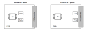
The location of the protection devices on the PCB is the simplest and most important circuit board reverse engineering rule to follow. The TVS devices should be located as close as possible to the noise source. In most systems, surge pulses occur on data and power lines that enter the PCB through the I/O connector. Below Figure provides an example of the recommended layout that places the TVS devices next to the connector.

Locating the TVS Devices Close to the I-O Connector in the process of Circuit Board Reverse Engineering
The length of the traces connecting the TVS devices, IC and I/O connector is a key factor that determines whether the surge currents are dissipated by the TVS devices or the IC’s internal ESD protection circuit. If the TVS diodes and internal IC protection circuit have a similar turn-on voltage, the only difference between the devices will be the impedance of their PCB traces.
A surge current will always follow the lowest impedance path; thus, the TVS should have a shorter trace than the IC, as shown in below Figure. A shorter trace length equates to smaller impedance, which helps ensure that the surge energy will be dissipated by the TVS device instead of the IC.

